Introduction to PCB-Stencil-Files
When ordering a printed circuit board (PCB) for your electronic project, it is essential to provide the manufacturer with the necessary files to ensure accurate fabrication and assembly. Among these files, PCB-Stencil-Files play a crucial role in the process of applying solder paste to the PCB during the surface mount technology (SMT) assembly process. In this article, we will discuss the various data files you need to upload with your PCB order, with a particular focus on PCB-Stencil-Files.
Types of Data Files for PCB Manufacturing
To ensure a smooth and accurate PCB manufacturing process, you need to provide your manufacturer with a set of data files that include all the necessary information about your PCB design. These files can be categorized into three main types:
- PCB Design Files
- Bill of Materials (BOM)
- PCB-Stencil-Files
Let’s explore each of these file types in more detail.
PCB Design Files
PCB design files contain the essential information needed to fabricate your PCB. These files are typically created using electronic design automation (EDA) software, such as Altium Designer, KiCad, or Eagle. The most common PCB design files include:
-
Gerber Files: These files contain the layer-by-layer information of your PCB design, including copper traces, solder mask, silkscreen, and drill holes. Gerber files are the industry standard for PCB fabrication and are essential for manufacturing your PCB.
-
ODB++ Files: ODB++ (Open Database++) is an alternative format to Gerber files that provides a more comprehensive and intelligent data package for PCB manufacturing. ODB++ files include not only the layer information but also the material stackup, drill data, and netlist information.
-
IPC-2581 Files: IPC-2581 is another data format that aims to provide a single, unified data file for PCB manufacturing. It includes all the necessary information for fabrication, assembly, and testing, making it a more efficient alternative to using multiple file formats.
Bill of Materials (BOM)
The Bill of Materials (BOM) is a comprehensive list of all the components required to assemble your PCB. It includes information such as the component reference designator, manufacturer part number, quantity, and description. The BOM is essential for the PCB Assembly process, as it ensures that the correct components are sourced and placed on the PCB.
When creating your BOM, it is important to adhere to the following best practices:
- Use a consistent format, such as a spreadsheet or CSV file
- Include all necessary component information (reference designator, manufacturer part number, quantity, description)
- Ensure that the component information matches the PCB design files
- Provide any additional notes or special instructions for the assembly process
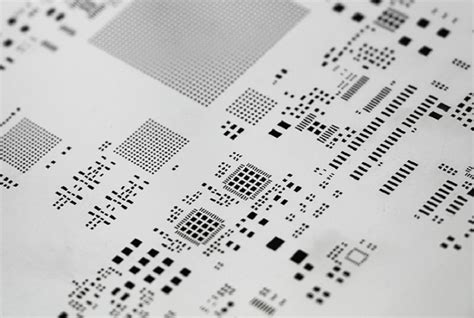
PCB-Stencil-Files
PCB-Stencil-Files are specifically designed for the solder paste application process during SMT assembly. A solder paste stencil is a thin metal sheet with apertures that correspond to the pads on your PCB. The stencil is placed over the PCB, and solder paste is applied using a squeegee, depositing the paste through the apertures onto the pads.
To create an accurate solder paste stencil, you need to provide your manufacturer with PCB-Stencil-Files. These files are derived from your PCB design files and contain information about the size, shape, and location of the apertures needed for solder paste application.
The most common PCB-Stencil-File formats include:
-
Gerber Files: Similar to PCB fabrication, Gerber files can be used to create solder paste stencils. These files contain the layer information for the top and bottom solder paste layers of your PCB.
-
ODB++ Files: ODB++ files can also be used for solder paste stencil creation, as they include the necessary solder paste layer information.
-
CAD Files: Some manufacturers may accept CAD files, such as DXF or DWG, for solder paste stencil creation. These files contain the outline and aperture information needed to cut the stencil.
When creating your PCB-Stencil-Files, consider the following guidelines:
- Ensure that the aperture sizes and locations match the pads on your PCB design files
- Provide the necessary stencil thickness information (typically 0.1 mm to 0.15 mm for standard SMT applications)
- Specify any special requirements, such as stepped stencils or custom aperture shapes

Best Practices for Uploading PCB-Stencil-Files
To ensure a smooth and accurate solder paste stencil fabrication process, follow these best practices when uploading your PCB-Stencil-Files:
-
Use the correct file format: Provide your files in a format that is compatible with your manufacturer’s requirements, such as Gerber, ODB++, or CAD files.
-
Include all necessary layers: Ensure that your files include the top and bottom solder paste layers, as well as any additional layers required for the stencil fabrication process.
-
Verify file accuracy: Double-check that your PCB-Stencil-Files match your PCB design files and BOM, ensuring that the apertures align with the component pads.
-
Provide clear instructions: Include any special requirements or instructions for the solder paste stencil fabrication process, such as stencil thickness, stepped stencils, or custom aperture shapes.
-
Compress and organize files: If uploading multiple files, compress them into a single archive (e.g., ZIP or RAR) and organize them in a clear and logical manner.
-
Communicate with your manufacturer: Maintain open communication with your PCB manufacturer throughout the process, clarifying any questions or concerns regarding your PCB-Stencil-Files.

Choosing the Right PCB Manufacturer
Selecting the right PCB manufacturer is crucial for ensuring the quality and reliability of your PCB assembly. When choosing a manufacturer, consider the following factors:
-
Experience and expertise: Look for a manufacturer with a proven track record in PCB fabrication and assembly, particularly in your specific industry or application.
-
Quality standards: Ensure that the manufacturer adheres to industry quality standards, such as IPC Class 2 or Class 3, depending on your project requirements.
-
Customer support: Choose a manufacturer that offers responsive and knowledgeable customer support, as this can be invaluable in resolving any issues or questions that may arise during the PCB manufacturing process.
-
Turnaround time: Consider the manufacturer’s turnaround time and whether it aligns with your project timeline and requirements.
-
Pricing: While cost is an important factor, avoid compromising on quality for the sake of lower prices. Look for a manufacturer that offers competitive pricing without sacrificing quality or reliability.

Frequently Asked Questions (FAQ)
-
What are the most common file formats for PCB-Stencil-Files?
The most common file formats for PCB-Stencil-Files are Gerber, ODB++, and CAD files (such as DXF or DWG). -
How do I ensure that my PCB-Stencil-Files match my PCB design files?
To ensure that your PCB-Stencil-Files match your PCB design files, verify that the aperture sizes and locations align with the component pads on your PCB. Double-check your files before submitting them to your manufacturer. -
What is the typical thickness for a solder paste stencil?
The typical thickness for a solder paste stencil ranges from 0.1 mm to 0.15 mm for standard SMT applications. However, the specific thickness may vary depending on your project requirements and the size of the components being used. -
Can I use the same PCB design files for PCB fabrication and solder paste stencil creation?
While PCB design files contain the necessary information for both PCB fabrication and solder paste stencil creation, you may need to generate separate files specifically for the stencil fabrication process. Consult with your PCB manufacturer to determine their specific requirements. -
What should I do if I have questions or concerns about my PCB-Stencil-Files?
If you have any questions or concerns about your PCB-Stencil-Files, reach out to your PCB manufacturer for assistance. Maintaining open communication throughout the PCB manufacturing process can help ensure a smooth and successful outcome.
Conclusion
Providing accurate and complete data files, including PCB-Stencil-Files, is essential for ensuring the quality and reliability of your PCB assembly. By understanding the different types of data files required, following best practices for creating and uploading your files, and choosing the right PCB manufacturer, you can streamline the PCB manufacturing process and achieve the best possible results for your electronic project.
Remember to maintain open communication with your manufacturer, ask questions when needed, and stay informed about the latest industry standards and best practices. By doing so, you can navigate the complexities of PCB manufacturing with confidence and bring your electronic designs to life.
| File Type | Description | Key Considerations |
|---|---|---|
| PCB Design Files | Contains layer-by-layer information for PCB fabrication (Gerber, ODB++, IPC-2581) | Ensure accurate and complete layer information |
| Bill of Materials (BOM) | Comprehensive list of components required for PCB assembly | Use consistent format and include all necessary component information |
| PCB-Stencil-Files | Specifically designed for solder paste application process (Gerber, ODB++, CAD) | Ensure aperture sizes and locations match PCB design files |
By providing these essential data files to your PCB manufacturer, you can ensure a smooth and successful PCB fabrication and assembly process, bringing your electronic designs to fruition.
No responses yet