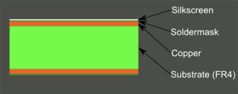
Introduction to PCB Silkscreen
PCB silkscreen, also known as legend or nomenclature, refers to the layer of text, numbers, and symbols printed on the surface of a printed circuit board (PCB). This information is essential for identifying components, understanding the board’s functionality, and facilitating the assembly process. In this comprehensive article, we’ll delve into the details of PCB silkscreen, its importance, the printing process, design considerations, and frequently asked questions.
The Importance of PCB Silkscreen
Component Identification
One of the primary functions of PCB silkscreen is to help identify components on the board. Each component is typically labeled with its reference designator, such as R1 for a resistor, C1 for a capacitor, or U1 for an integrated circuit. This labeling makes it easier for engineers, technicians, and manufacturers to locate and work with specific components during assembly, testing, and troubleshooting.
Orientation and Polarity Indicators
Silkscreen markings also provide critical information about Component orientation and polarity. Many components, such as diodes, electrolytic capacitors, and ICs, have specific orientation requirements. Silkscreen symbols, such as a notch or a dot, indicate the correct placement and orientation of these components, preventing assembly errors that could lead to malfunctions or damage.
Test Points and Debugging
PCB silkscreen often includes labels for test points, which are used for probing and debugging the circuit. These labels help technicians quickly identify where to connect test equipment, such as oscilloscopes or multimeters, to measure voltages, currents, or signals. Clear and accurate labeling of test points can significantly speed up the debugging process and reduce the likelihood of errors.
Branding and Aesthetics
In addition to its functional purposes, PCB silkscreen can also be used for branding and aesthetic purposes. Company logos, product names, or decorative elements can be incorporated into the silkscreen design to create a professional and visually appealing product. However, it’s essential to ensure that any decorative elements do not interfere with the readability of functional silkscreen markings.

The PCB Silkscreen Printing Process
Screen Printing
The most common method for applying silkscreen to a PCB is screen printing. In this process, a fine mesh screen is stretched over a frame, and a stencil is created on the screen with the desired silkscreen design. Ink is then applied to the screen and forced through the open areas of the stencil onto the PCB surface using a squeegee. This process is repeated for each color used in the silkscreen design.
Ink Selection
The choice of ink is crucial for creating durable and readable silkscreen markings. The most common inks used for PCB silkscreen are epoxy-based or UV-curable. These inks are designed to withstand the high temperatures and chemicals used in the PCB manufacturing process, ensuring that the markings remain legible throughout the board’s life. White ink is the most popular choice for silkscreen, as it provides excellent contrast against the typical green or black Solder Mask.
Curing and Drying
After the ink is applied to the PCB surface, it must be cured or dried to ensure proper adhesion and durability. For epoxy-based inks, this typically involves baking the PCB in an oven at a specific temperature and duration. UV-curable inks, on the other hand, are exposed to ultraviolet light, which triggers a rapid curing process. Once cured, the silkscreen markings should be resistant to abrasion, chemicals, and high temperatures.

PCB Silkscreen Design Considerations
Readability and Font Selection
When designing PCB silkscreen, readability should be a top priority. Choose fonts that are clear, legible, and appropriate for the size of the components and the overall board. Sans-serif fonts, such as Arial or Helvetica, are often preferred for their simplicity and readability at small sizes. Avoid using overly decorative or complex fonts that may be difficult to read, especially when printed on the small surface area of a PCB.
Size and Spacing
To ensure that silkscreen markings are easily readable, it’s essential to consider the size and spacing of the text and symbols. The minimum recommended text height for PCB silkscreen is 0.8mm (0.032 inches), although larger sizes may be necessary for better visibility. Maintain adequate spacing between letters, words, and symbols to prevent crowding and improve legibility. It’s also crucial to keep silkscreen markings away from component pads and other critical board features to avoid interference with the assembly process.
Color and Contrast
As mentioned earlier, white is the most common color for PCB silkscreen due to its excellent contrast against green or black solder masks. However, other colors, such as yellow or black, may be used for specific applications or to differentiate between different types of information. When selecting colors, always consider the contrast between the silkscreen and the background to ensure optimal readability.
Placement and Orientation
When placing silkscreen markings on the PCB, consider the orientation of the components and the overall board. Text and symbols should be oriented in a way that is easily readable when the board is installed in its final application. For components with specific orientation requirements, such as ICs or connectors, place the silkscreen markings close to the component and aligned with its orientation to minimize the risk of assembly errors.
Silkscreen Layer in PCB Design Software
Most PCB design software packages include a dedicated silkscreen layer that allows designers to create and place silkscreen markings. This layer is typically labeled as “Silk”, “Silkscreen”, or “Legend” and is separate from the copper and solder mask layers. When creating silkscreen designs, be sure to adhere to the design rules and guidelines specified by your PCB Manufacturer to ensure compatibility with their processes and requirements.

Frequently Asked Questions (FAQ)
1. Is silkscreen required on every PCB?
While silkscreen is not strictly required on every PCB, it is highly recommended for most applications. The information provided by silkscreen markings is essential for component identification, assembly, and troubleshooting. In some cases, such as very simple or low-cost boards, silkscreen may be omitted to reduce manufacturing costs. However, for the majority of PCBs, the benefits of silkscreen far outweigh the minimal additional cost.
2. Can silkscreen markings be placed on both sides of a PCB?
Yes, silkscreen markings can be placed on both sides of a PCB. This is particularly useful for double-sided boards or those with components on both the top and bottom surfaces. When designing silkscreen for double-sided boards, ensure that the markings on each side are mirror-imaged to maintain readability when the board is flipped over.
3. How durable are silkscreen markings?
When printed with the appropriate inks and properly cured, silkscreen markings are highly durable and resistant to abrasion, chemicals, and high temperatures. Epoxy-based and UV-curable inks are specifically formulated to withstand the rigors of the PCB manufacturing process and the board’s intended operating environment. However, it’s essential to handle PCBs with care to avoid scratching or damaging the silkscreen markings.
4. Can silkscreen markings be customized with logos or graphics?
Yes, silkscreen markings can be customized to include logos, graphics, or other decorative elements. However, it’s essential to ensure that any custom graphics do not interfere with the readability of functional silkscreen markings, such as component labels or orientation indicators. When incorporating logos or graphics, work closely with your PCB manufacturer to ensure that the designs are compatible with their silkscreen printing process and guidelines.
5. Are there any alternatives to traditional silkscreen printing for PCBs?
While screen printing is the most common method for applying silkscreen to PCBs, there are a few alternatives available. One option is direct legend printing (DLP), which uses a specialized inkjet printer to apply the silkscreen markings directly onto the PCB surface. This method allows for greater flexibility in design and can be more cost-effective for low-volume production runs. Another alternative is laser marking, which uses a laser to etch the silkscreen markings onto the PCB surface. This method is highly durable and precise but may be more expensive than traditional screen printing.
Conclusion
PCB silkscreen is a crucial element of printed circuit board design and manufacturing, providing essential information for component identification, assembly, and troubleshooting. By understanding the importance of silkscreen, the printing process, and key design considerations, engineers and designers can create PCBs that are functional, reliable, and user-friendly. When designing silkscreen markings, prioritize readability, clarity, and compatibility with the intended manufacturing process to ensure the best possible results.
| Advantage | Description |
|---|---|
| Component Identification | Silkscreen markings help identify components on the PCB, making assembly and troubleshooting easier. |
| Orientation and Polarity Indicators | Symbols and markings indicate the correct orientation and polarity of components, preventing assembly errors. |
| Test Points and Debugging | Labels for test points facilitate probing and debugging of the circuit. |
| Branding and Aesthetics | Silkscreen can incorporate logos, product names, or decorative elements for a professional appearance. |
By following best practices and working closely with PCB manufacturers, designers can create silkscreen markings that enhance the functionality, reliability, and overall quality of their printed circuit boards.
No responses yet