What is a Stencil and Why is it Important in SMT Assembly?
In Surface Mount Technology (SMT) assembly, a stencil is a thin sheet of metal or other material with cut-out openings that correspond to the pad locations on a Printed Circuit Board (PCB). The stencil is used to apply solder paste onto the PCB pads before the components are placed. This process ensures precise and consistent solder paste deposition, which is crucial for achieving reliable solder joints and overall assembly quality.
Stencils play a vital role in the SMT assembly process for several reasons:
- Precise solder paste deposition: Stencils allow for accurate and consistent solder paste application onto the PCB pads. The openings in the stencil are designed to match the size and shape of the pads, ensuring that the right amount of solder paste is deposited in the correct locations.
- Increased efficiency: Using a stencil for solder paste application is much faster and more efficient than manual methods. This is particularly important in high-volume production, where speed and consistency are critical.
- Improved quality: Consistent solder paste deposition leads to better solder joint quality and fewer defects. This, in turn, results in higher overall assembly quality and reliability.
- Accommodation of fine-pitch components: As electronic devices become smaller and more complex, the use of fine-pitch components (components with very small lead spacing) has increased. Stencils enable the precise application of solder paste for these components, which would be difficult or impossible to achieve with manual methods.
Types of Stencils
There are several types of stencils used in SMT assembly, each with its own characteristics and applications. The most common types include:
- Laser-Cut Stencils: These stencils are made by using a laser to cut the openings in a thin sheet of stainless steel. Laser-cut stencils are known for their precision and durability, making them suitable for high-volume production and fine-pitch applications.
- Electroformed stencils: Electroformed stencils are created by electroplating nickel onto a photoresist-coated master. The photoresist is then removed, leaving a thin nickel stencil with the desired openings. These stencils are known for their high detail and accuracy, making them ideal for very fine-pitch applications and small apertures.
- Additive stencils: Additive stencils, also known as E-FAB or Nano-Coat stencils, are made by selectively depositing a polymer coating onto a fine mesh screen. The coating is then cured, creating a stencil with the desired openings. Additive stencils are suitable for applications that require very fine features or unusual aperture shapes.
- Hybrid stencils: Hybrid stencils combine different manufacturing techniques, such as laser cutting and electroforming, to create a single stencil. This approach allows for the benefits of each technique to be utilized in specific areas of the stencil, depending on the requirements of the PCB design.
Factors Affecting Stencil Design
When designing a stencil for SMT assembly, several factors must be considered to ensure optimal performance:
- Aperture size and shape: The size and shape of the stencil openings (apertures) should match the size and shape of the PCB pads. This ensures that the correct amount of solder paste is deposited and that the paste is evenly distributed across the pad.
- Stencil thickness: The thickness of the stencil determines the volume of solder paste deposited onto the pads. Thicker stencils deposit more paste, while thinner stencils deposit less. The optimal thickness depends on the size and pitch of the components being used.
- Aperture wall angle: The angle of the aperture walls can affect the release of the solder paste from the stencil. A slightly tapered wall (usually 5-7 degrees) helps the paste release more easily and prevents clogging.
- Aperture aspect ratio: The aspect ratio is the relationship between the width and thickness of the aperture. A higher aspect ratio (smaller width relative to thickness) can make it more difficult for the solder paste to release from the stencil. It’s important to maintain an appropriate aspect ratio to ensure good paste release and prevent clogging.
- Area ratio: The area ratio is the relationship between the area of the aperture opening and the area of the aperture walls. A higher area ratio (larger opening relative to wall area) promotes better paste release. It’s important to maintain a minimum area ratio (usually 0.66) to ensure good paste release and prevent clogging.
- Stencil material: The choice of stencil material can affect its durability, performance, and cost. Stainless steel is the most common material for laser-cut stencils, while nickel is used for electroformed stencils. The material should be compatible with the solder paste being used and resist wear and damage.

Stencil-Making Process
The process of making a stencil involves several steps, which may vary depending on the type of stencil being created. Here’s a general overview of the stencil-making process for laser-cut stencils:
- Design creation: The stencil design is created using CAD software, based on the PCB layout and the factors discussed in the previous section. The design includes the aperture sizes, shapes, and locations, as well as any necessary fiducials or markings.
- Material selection: The appropriate stainless steel sheet is selected based on the required stencil thickness and size.
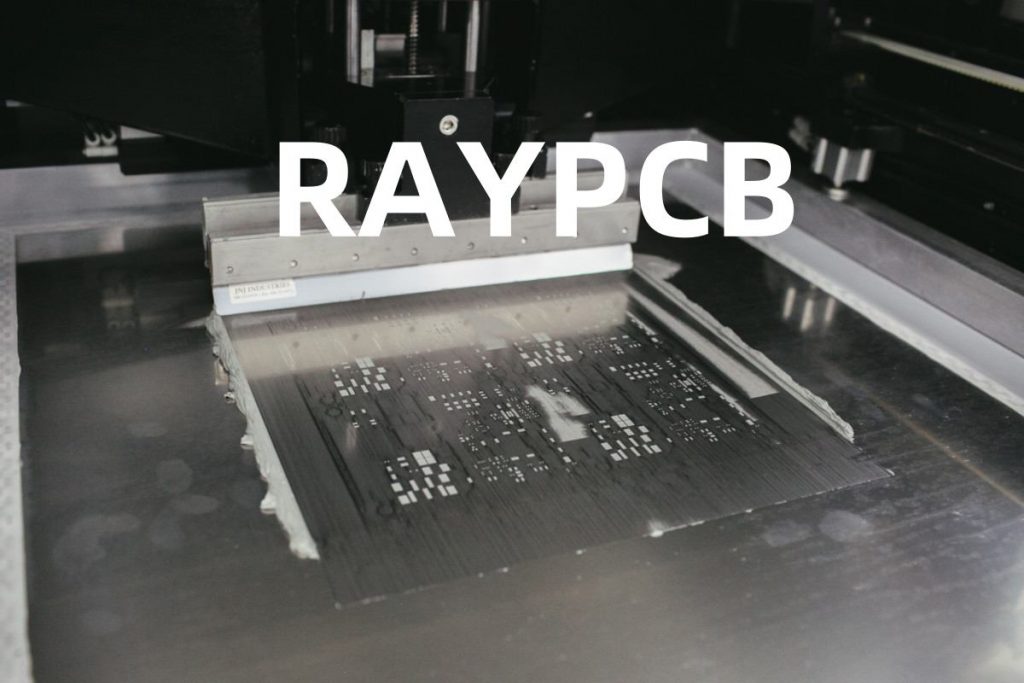
- Laser cutting: The stencil design is loaded into a laser cutting machine, which uses a high-powered laser to cut the apertures into the stainless steel sheet. The laser follows the design, creating precise openings that match the PCB pads.
- Deburring and cleaning: After laser cutting, the stencil undergoes a deburring process to remove any rough edges or burrs from the apertures. This ensures smooth solder paste release and prevents clogging. The stencil is then cleaned to remove any debris or contaminants.
- Inspection: The finished stencil is inspected to ensure that all apertures are cut correctly and that there are no defects or irregularities. This may involve visual inspection, as well as using specialized measurement tools to verify aperture dimensions and locations.
- Packaging and shipping: Once the stencil has passed inspection, it is packaged and shipped to the customer, ready for use in the SMT assembly process.
For other types of stencils, such as electroformed or additive stencils, the process may differ slightly, but the general principles of design creation, material selection, aperture creation, and inspection still apply.

Advantages and Disadvantages of Different Stencil Types
Each type of stencil has its own advantages and disadvantages, which should be considered when selecting the most appropriate stencil for a given application.
Laser-Cut Stencils
Advantages:
– High precision and repeatability
– Durable and long-lasting
– Suitable for a wide range of aperture sizes and shapes
– Cost-effective for high-volume production
Disadvantages:
– Limited minimum aperture size (around 0.3mm)
– Slightly tapered aperture walls may affect paste release
– Higher initial cost compared to other types
Electroformed Stencils
Advantages:
– Excellent detail and accuracy
– Capable of very fine apertures (down to 0.1mm)
– Smooth aperture walls for optimal paste release
– Suitable for fine-pitch and ultra-fine-pitch applications
Disadvantages:
– Higher cost compared to laser-cut stencils
– Less durable than stainless steel stencils
– Limited maximum stencil size
Additive Stencils
Advantages:
– Capable of very fine apertures and complex shapes
– Smooth aperture walls for optimal paste release
– Suitable for fine-pitch and ultra-fine-pitch applications
– Lower cost compared to electroformed stencils
Disadvantages:
– Limited durability compared to metal stencils
– May require more frequent cleaning and maintenance
– Limited maximum stencil size
Hybrid Stencils
Advantages:
– Combines the benefits of multiple stencil types
– Can optimize performance for specific areas of the PCB
– Suitable for complex PCB designs with varying requirements
Disadvantages:
– Higher cost compared to single-type stencils
– More complex design and manufacturing process
– May require more lead time for production
Ultimately, the choice of stencil type depends on the specific requirements of the PCB design, the components being used, the production volume, and the budget available.
How to Make Holes in SMT Stencils
Making holes, or apertures, in SMT stencils is a crucial part of the stencil-making process. The method used to create these holes depends on the type of stencil being manufactured.
Laser Cutting
For laser-cut stencils, holes are made using a high-powered laser that follows the stencil design. The laser vaporizes the stainless steel material, creating precise openings that match the size and shape of the PCB pads. The laser cutting process involves several steps:
- The stencil design file is loaded into the laser cutting machine’s software.
- The stainless steel sheet is placed on the machine bed and secured in place.
- The laser head moves across the sheet, following the design and cutting the apertures.
- The process is repeated until all apertures have been cut.
- The stencil is removed from the machine and undergoes deburring and cleaning.
Laser cutting is a highly precise and repeatable method for creating apertures, capable of achieving aperture sizes down to around 0.3mm.
Electroforming
Electroformed stencils are created using a photolithography process, followed by electroplating. The apertures are formed by selectively exposing a photoresist-coated master to light, which hardens the exposed areas. The unexposed areas are then removed, leaving a negative image of the stencil design. This master is then used as a mold for electroplating nickel onto the surface, creating the final stencil with the desired apertures.
The electroforming process allows for very fine apertures (down to 0.1mm) and smooth aperture walls, making it ideal for fine-pitch and ultra-fine-pitch applications.
Additive Manufacturing
Additive stencils, or E-FAB stencils, are created by selectively depositing a polymer coating onto a fine mesh screen. The coating is applied using a special printing process, which deposits the polymer only in the areas where apertures are desired. The coating is then cured, creating a stencil with the designed apertures.
Additive manufacturing allows for very fine apertures and complex aperture shapes, as the polymer coating can be applied in intricate patterns. This process is suitable for fine-pitch and ultra-fine-pitch applications, as well as for PCBs with unusual pad shapes or sizes.
Regardless of the method used, the goal is to create precise, clean, and consistent apertures that will allow for optimal solder paste deposition during the SMT assembly process.
Frequently Asked Questions (FAQ)
- What is the minimum aperture size that can be achieved with laser-cut stencils?
Laser-cut stencils can typically achieve aperture sizes down to around 0.3mm (12 mil). For smaller apertures, electroformed or additive stencils may be necessary. - How does stencil thickness affect solder paste deposition?
Stencil thickness directly affects the volume of solder paste deposited onto the PCB pads. Thicker stencils deposit more paste, while thinner stencils deposit less. The optimal thickness depends on the size and pitch of the components being used, as well as the desired solder joint profile. - What is the purpose of aperture wall tapering in laser-cut stencils?
Aperture wall tapering, usually around 5-7 degrees, helps to improve solder paste release from the stencil. The slight angle prevents the paste from sticking to the walls and ensures a clean release onto the PCB pads. - How often should stencils be cleaned during the SMT assembly process?
Stencils should be cleaned regularly to prevent solder paste buildup and ensure consistent paste deposition. The frequency of cleaning depends on factors such as the type of solder paste being used, the production volume, and the stencil design. A general guideline is to clean the stencil every 4-8 hours of continuous use, or whenever print quality begins to deteriorate. - Can damaged stencils be repaired, or must they be replaced?
In some cases, minor damage to stencils can be repaired using specialized techniques, such as laser welding or micro-TIG welding. However, the feasibility of repair depends on the extent and location of the damage. If the damage is severe or affects critical apertures, it may be necessary to replace the stencil to ensure optimal performance and print quality.
| Stencil Type | Minimum Aperture Size | Typical Thickness Range | Aperture Wall Angle | Material |
|---|---|---|---|---|
| Laser-cut | 0.3mm (12 mil) | 0.1mm – 0.3mm (4-12 mil) | 5-7 degrees | Stainless Steel |
| Electroformed | 0.1mm (4 mil) | 0.05mm – 0.15mm (2-6 mil) | Near 90 degrees | Nickel |
| Additive | 0.1mm (4 mil) | 0.05mm – 0.15mm (2-6 mil) | Near 90 degrees | Polymer |
In conclusion, making holes, or apertures, in SMT stencils is a critical aspect of the stencil-making process. The method used depends on the type of stencil being manufactured, with laser cutting, electroforming, and additive manufacturing being the most common techniques. Each method has its own advantages and limitations, and the choice ultimately depends on the specific requirements of the PCB design and assembly process.
By understanding the factors that affect stencil design, such as aperture size, shape, and wall angle, as well as the pros and cons of different stencil types, engineers and manufacturers can select the most appropriate stencil for their needs. This, in turn, ensures optimal solder paste deposition, high-quality solder joints, and reliable SMT assembly.
No responses yet