Introduction to PCB Design
Printed Circuit Boards (PCBs) are an essential component of modern electronics. They provide a platform for mounting and connecting electronic components to create functional circuits. PCBs are used in a wide range of applications, from simple hobby projects to complex industrial systems. In the past, designing and manufacturing PCBs required specialized knowledge and expensive equipment. However, with the advent of online PCB design tools and services, it has become easier than ever for individuals and small businesses to create their own custom PCBs.
In this article, we will explore the world of online PCB design and how you can use these tools to create your own PCBs. We will cover the basics of PCB design, the advantages of online PCB design tools, and the steps involved in creating a PCB using these tools. We will also provide some tips and best practices for designing high-quality PCBs that meet your specific requirements.
What is a PCB?
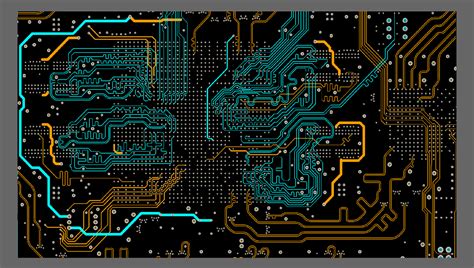
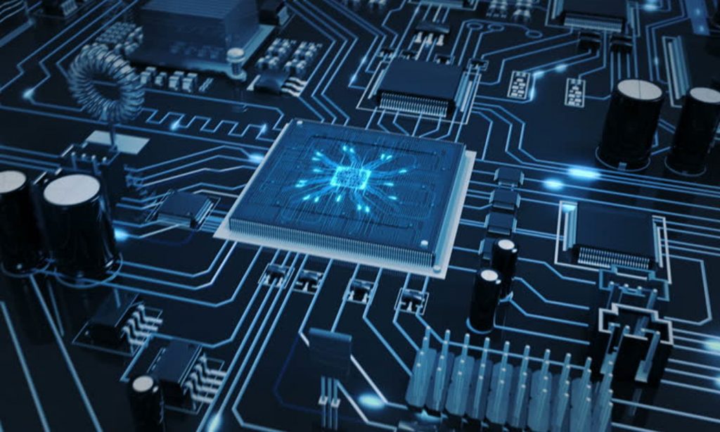
A PCB is a flat board made of insulating material, typically fiberglass or composite epoxy, with conductive copper traces printed on its surface. These traces connect the various electronic components mounted on the board, such as resistors, capacitors, integrated circuits, and connectors. PCBs provide a stable and reliable platform for these components, allowing them to function as intended.
PCBs come in various sizes, shapes, and configurations, depending on the specific application. They can be single-sided, with copper traces on only one side of the board, or double-sided, with traces on both sides. Some PCBs even have multiple layers, with conductive traces sandwiched between insulating layers.
The main advantages of using PCBs over other methods of circuit construction, such as point-to-point wiring or breadboarding, include:
- Improved reliability and durability
- Reduced size and weight
- Easier assembly and maintenance
- Lower manufacturing costs for high volumes

Why Use Online PCB Design Tools?
Traditionally, PCB design required specialized software and hardware, such as CAD programs and plotters. These tools were expensive and required a steep learning curve, making them inaccessible to most individuals and small businesses. However, with the rise of online PCB design tools, creating custom PCBs has become much more accessible and affordable.
Online PCB design tools are web-based applications that allow users to create PCB layouts using a simple graphical interface. These tools typically include a library of common electronic components and footprints, as well as tools for drawing traces, placing components, and generating manufacturing files.
The main advantages of using online PCB design tools include:
- Accessibility: Online tools can be accessed from any computer with an internet connection, without the need for specialized software or hardware.
- Ease of use: Most online tools have a user-friendly interface and do not require extensive technical knowledge or experience.
- Affordability: Many online tools offer free or low-cost plans, making them accessible to individuals and small businesses on a budget.
- Collaboration: Some online tools allow multiple users to work on the same project simultaneously, facilitating collaboration and teamwork.
- Rapid prototyping: Online tools can generate manufacturing files quickly, allowing for faster prototyping and iteration.

Steps for Creating a PCB Using Online Tools
Creating a PCB using online tools typically involves the following steps:
- Define your requirements: Before starting your design, you need to have a clear idea of what your PCB needs to do. This includes the number and type of components, the size and shape of the board, and any special features or constraints.
- Choose an online PCB design tool: There are many online PCB design tools available, each with its own features and pricing. Some popular options include EasyEDA, Upverter, and CircuitMaker. Choose a tool that meets your needs and budget.
- Create a schematic: The first step in designing a PCB is to create a schematic diagram of your circuit. This involves placing the components and connecting them with virtual wires. Most online tools have a library of common components that you can drag and drop onto your schematic.
- Design the PCB layout: Once your schematic is complete, you can convert it into a PCB layout. This involves arranging the components on the board and drawing the copper traces that will connect them. Online tools typically have automated routing features that can help with this process, but you may need to make manual adjustments to optimize your layout.
- Generate manufacturing files: After your PCB layout is complete, you need to generate the files that will be used to manufacture the board. These typically include Gerber files (for the copper layers and drill holes) and a bill of materials (BOM) listing the components used. Most online tools can generate these files automatically.
- Order your PCB: Once you have your manufacturing files, you can send them to a PCB fabrication service to have your board manufactured. Many online PCB design tools have integrated ordering features that allow you to get quotes and place orders directly from the tool.
Tips for Designing High-Quality PCBs
Designing a high-quality PCB requires attention to detail and adherence to best practices. Here are some tips to help you create PCBs that are reliable, efficient, and manufacturable:
- Keep your traces as short and direct as possible to minimize signal loss and interference.
- Use appropriate trace widths and spacing for the current and voltage requirements of your circuit.
- Avoid acute angles in your traces, as they can cause manufacturing issues. Use 45-degree angles instead.
- Place decoupling capacitors close to the power pins of ICs to reduce noise and improve power stability.
- Use ground planes to provide a low-impedance return path for signals and reduce electromagnetic interference (EMI).
- Follow the manufacturer’s recommended footprints and layouts for your components to ensure proper fit and functionality.
- Use a consistent naming and labeling scheme for your components and nets to avoid confusion and errors.
- Perform a design rule check (DRC) before generating your manufacturing files to catch any errors or violations.
Common PCB Design Mistakes to Avoid
Even with the best tools and practices, it’s easy to make mistakes when designing a PCB. Here are some common pitfalls to watch out for:
- Incorrect component orientation: Make sure your components are oriented correctly on the board, especially polarized components like electrolytic capacitors and diodes.
- Insufficient clearance: Ensure that there is enough space between components and traces to avoid short circuits and manufacturing issues.
- Incorrect hole sizes: Make sure the drill holes for your components are the correct size and shape for the leads or pins.
- Incorrect layer stackup: If your PCB has multiple layers, make sure they are arranged in the correct order and with the proper insulation between them.
- Incomplete or incorrect net names: Make sure all your nets are properly named and connected in your schematic and layout.
- Forgetting to specify the correct PCB thickness and copper weight when ordering your board.
PCB Design Tools Comparison
To help you choose the right online PCB design tool for your needs, here is a comparison of some popular options:
| Tool | Free Plan | Paid Plans | Integrated Ordering | Collaboration |
|---|---|---|---|---|
| EasyEDA | Yes | Yes | Yes | Yes |
| Upverter | Yes | Yes | No | Yes |
| CircuitMaker | Yes | No | No | Yes |
| PCBWeb | Yes | Yes | Yes | No |
| Fritzing | Yes | No | No | No |
FAQ
- Q: Do I need prior experience to use online PCB design tools?
A: No, most online PCB design tools are designed to be user-friendly and do not require extensive technical knowledge or experience. However, having a basic understanding of electronics and PCB design principles can be helpful. - Q: How much does it cost to have a PCB manufactured?
A: The cost of manufacturing a PCB depends on various factors such as the size and complexity of the board, the number of layers, and the quantity ordered. Prices can range from a few dollars for simple, small-quantity boards to hundreds of dollars for complex, high-volume orders. - Q: How long does it take to receive a manufactured PCB?
A: The turnaround time for PCB manufacturing varies depending on the service provider and the complexity of the board. Some providers offer expedited services that can deliver boards in as little as 24 hours, while others may take several weeks for standard orders. - Q: Can I use online PCB design tools for commercial projects?
A: Yes, many online PCB design tools allow commercial use, although some may require a paid subscription or license for commercial projects. Be sure to check the terms of service and licensing agreements of the tool you choose. - Q: Are there any limitations to using online PCB design tools compared to traditional software?
A: Online PCB design tools may have some limitations compared to traditional desktop software, such as reduced customization options or limited library components. However, for most common PCB design tasks, online tools are more than sufficient and offer the added benefits of accessibility, collaboration, and rapid prototyping.
Conclusion
Online PCB design tools have revolutionized the way individuals and small businesses create custom PCBs. These tools offer accessibility, ease of use, and affordability, making it possible for anyone with a basic understanding of electronics to design and manufacture their own PCBs.
By following the steps outlined in this article and adhering to best practices and common pitfalls, you can create high-quality PCBs that meet your specific requirements. Whether you are a hobbyist working on a personal project or a small business owner prototyping a new product, online PCB design tools provide a powerful and flexible platform for bringing your ideas to life.
As with any new tool or skill, designing PCBs using online tools may require some learning and experimentation. However, with practice and persistence, you can master the art of PCB design and unlock new possibilities for your electronic projects. So why not give it a try and see what you can create?
No responses yet