Introduction to PCB Manufacturing
Printed Circuit Board (PCB) manufacturing is a crucial process in the electronics industry, enabling the creation of complex electronic devices and systems. PCBs provide a platform for interconnecting electronic components, such as resistors, capacitors, and integrated circuits, allowing them to function together as a complete electronic system. The manufacturing process involves several stages, from design and layout to fabrication and assembly, each requiring precise control and attention to detail to ensure the highest quality end product.
In this article, we will explore the various aspects of PCB manufacturing, including the types of PCBs, the manufacturing process, and the capabilities of modern PCB fabrication and assembly facilities. We will also discuss the importance of choosing the right PCB manufacturer and the factors to consider when making this decision.
Types of PCBs
There are several types of PCBs, each designed to meet specific requirements and applications. The most common types include:
Single-Layer PCBs
Single-layer PCBs, also known as single-sided PCBs, have conductive traces on only one side of the substrate. These boards are the simplest and most cost-effective to manufacture, making them ideal for basic electronic projects and low-density designs.
Double-Layer PCBs
Double-layer PCBs, or double-sided PCBs, have conductive traces on both sides of the substrate, allowing for higher component density and more complex designs compared to single-layer boards. The two layers are connected using through-hole vias, which are small holes drilled through the board and plated with conductive material.
Multi-Layer PCBs
Multi-layer PCBs consist of three or more conductive layers, separated by insulating layers. These boards offer the highest component density and design complexity, making them suitable for advanced electronic applications, such as smartphones, computers, and medical devices. The layers are interconnected using through-hole vias and blind or buried vias, which are partially drilled holes that connect inner layers without reaching the surface of the board.
Flexible PCBs
Flexible PCBs, or flex PCBs, are made using a flexible substrate, such as polyimide or polyester, allowing the board to bend and conform to various shapes. These boards are commonly used in applications that require flexibility, such as wearable electronics, robotics, and aerospace systems.
Rigid-Flex PCBs
Rigid-flex PCBs combine the benefits of both rigid and flexible PCBs, featuring rigid sections for mounting components and flexible sections for connecting multiple rigid boards or conforming to irregular shapes. This type of PCB is often used in applications that require high reliability and space savings, such as medical devices, automotive electronics, and military equipment.

The PCB Manufacturing Process
The PCB manufacturing process consists of several stages, each contributing to the creation of a high-quality, reliable printed circuit board. The main stages include:
PCB Design and Layout
The first stage in PCB manufacturing is the design and layout of the board. This process involves creating a schematic diagram that represents the electrical connections between components, followed by the physical layout of the components and conductive traces on the board. PCB design software, such as Altium Designer, Eagle, or KiCad, is used to create the schematic and layout files, which are then sent to the PCB manufacturer for fabrication.
PCB Fabrication
The PCB fabrication process begins with the creation of the substrate, which is typically made of FR-4, a flame-retardant glass-reinforced epoxy laminate. The substrate is cut to the desired size and shape, and copper foil is laminated onto one or both sides of the board, depending on the type of PCB being manufactured.
Next, the conductive traces are created using a photolithography process. A photoresist layer is applied to the copper foil, and the desired trace pattern is transferred onto the photoresist using UV light exposure through a photomask. The exposed photoresist is then developed, and the unwanted copper is etched away using a chemical solution, leaving only the desired conductive traces.
After etching, the remaining photoresist is removed, and the board is inspected for defects. If the board passes inspection, it moves on to the drilling stage, where holes are drilled for through-hole components and vias. The holes are then plated with a conductive material, typically copper, to ensure electrical connectivity between layers.
Finally, a soldermask layer is applied to the board, which serves as an insulating and protective layer, exposing only the areas where components will be soldered. A silkscreen layer is also added, which includes text and symbols to aid in the assembly process and provide information about the board’s components and functions.
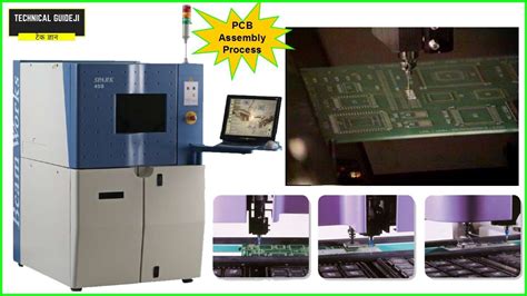
PCB Assembly
Once the PCB fabrication process is complete, the board moves on to the assembly stage. There are two main methods of PCB assembly: through-hole assembly and surface mount assembly.
Through-Hole Assembly
Through-hole assembly involves inserting component leads through the drilled holes in the board and soldering them to the conductive traces on the opposite side. This method is typically used for larger components or those that require higher mechanical stability.
Surface Mount Assembly
Surface mount assembly, or SMT assembly, involves placing components directly onto the surface of the board and soldering them to the conductive traces using a reflow soldering process. SMT Components are smaller and have shorter leads compared to through-hole components, allowing for higher component density and smaller board sizes.
The PCB assembly process typically involves the following steps:
- Solder paste application: A precise amount of solder paste is applied to the pads on the board using a stencil or screen printing process.
- Component placement: The SMT components are placed onto the solder paste using a pick-and-place machine, which accurately positions the components based on the design files.
- Reflow soldering: The board is passed through a reflow oven, which heats the solder paste to its melting point, allowing it to form a strong bond between the components and the conductive traces.
- Inspection and testing: The assembled board is inspected for defects, such as bridging, solder joint issues, or misaligned components. Electrical tests are also performed to ensure the board functions as intended.

Choosing the Right PCB Manufacturer
Selecting the right PCB manufacturer is crucial to ensuring the success of your electronic project. When choosing a manufacturer, consider the following factors:
Manufacturing Capabilities
Ensure that the manufacturer has the necessary equipment and expertise to fabricate and assemble the type of PCB your project requires. This includes the ability to handle the desired board size, layer count, material, and component types.
Quality Control
A reputable PCB manufacturer should have strict quality control processes in place to ensure the consistency and reliability of their products. Look for certifications such as ISO 9001, IPC Class 2 or 3, and UL listing, which demonstrate the manufacturer’s commitment to quality.
Lead Time and Pricing
Consider the manufacturer’s lead time and pricing structure to ensure they align with your project’s timeline and budget. Keep in mind that faster lead times and lower prices may sometimes come at the cost of quality, so it’s essential to find a balance that meets your needs.
Customer Support and Communication
Choose a manufacturer that provides excellent customer support and communicates effectively throughout the manufacturing process. This includes providing timely updates, addressing concerns, and offering technical assistance when needed.

PCB Manufacturing Capabilities
Modern PCB manufacturing facilities offer a wide range of capabilities to meet the diverse needs of electronic projects across various industries. Some of the key capabilities include:
High Density Interconnect (HDI) PCBs
HDI PCBs feature finer trace widths, smaller vias, and higher component density compared to traditional PCBs. These boards are essential for applications that require miniaturization, such as smartphones, wearables, and IoT devices. HDI manufacturing capabilities include microvias, blind and buried vias, and fine-pitch SMT assembly.
Controlled Impedance PCBs
Controlled impedance PCBs are designed to maintain a specific impedance value along the conductive traces, which is critical for high-speed digital and RF applications. PCB manufacturers with controlled impedance capabilities can precisely control the trace width, spacing, and dielectric thickness to achieve the desired impedance characteristics.
Heavy Copper PCBs
Heavy copper PCBs feature thicker copper layers, typically ranging from 4 oz to 20 oz per square foot, compared to the standard 1 oz to 2 oz used in most PCBs. These boards are used in power electronics applications, such as motor drives, inverters, and power supplies, where high current carrying capacity is required. Manufacturing heavy copper PCBs requires specialized equipment and processes to ensure proper adhesion and plating of the thick copper layers.
Rigid-Flex PCBs
As mentioned earlier, rigid-flex PCBs combine rigid and flexible sections to offer unique benefits in terms of reliability, space savings, and design flexibility. Manufacturing rigid-flex PCBs requires expertise in handling and bonding the different materials, as well as precise control over the transition zones between the rigid and flexible sections.
Advanced Materials
PCB manufacturers with advanced material capabilities can work with a variety of substrates and laminates to meet specific performance requirements. This includes high-frequency materials, such as Rogers and Isola, for RF and microwave applications, as well as thermally conductive materials for improved heat dissipation in high-power applications.
PCB Assembly Capabilities
In addition to PCB fabrication capabilities, modern PCB assembly facilities offer a range of services to streamline the production process and ensure high-quality end products. Some of the key PCB assembly capabilities include:
Automated Optical Inspection (AOI)
AOI systems use high-resolution cameras and advanced image processing algorithms to inspect assembled PCBs for defects, such as missing components, incorrect polarity, or solder joint issues. This automated inspection process is faster and more reliable than manual inspection, ensuring higher quality and consistency in the final product.
X-Ray Inspection
X-ray inspection systems are used to inspect solder joints and other internal features of assembled PCBs that are not visible from the surface. This is particularly important for BGAs, QFNs, and other packages with hidden solder joints. X-ray inspection can detect issues such as voids, bridging, or insufficient solder, ensuring the reliability of the assembled board.
Functional Testing
Functional testing involves verifying the electrical performance of the assembled PCB to ensure it meets the design specifications. This can include in-circuit testing (ICT), flying probe testing, or boundary scan testing, depending on the complexity of the board and the available test points. Functional testing helps identify any issues related to component functionality, signal integrity, or overall board performance.
Conformal Coating
Conformal coating is a process that involves applying a protective layer onto the assembled PCB to shield it from environmental factors such as moisture, dust, or chemical contaminants. PCB assembly facilities with conformal coating capabilities can apply various types of coatings, such as acrylic, silicone, or polyurethane, depending on the specific requirements of the application.
Box Build and System Integration
Some PCB assembly facilities offer box build and system integration services, which involve assembling the completed PCBs into enclosures, along with other components such as displays, connectors, and wiring harnesses. This turnkey solution simplifies the production process for OEMs, allowing them to receive a fully assembled and tested product ready for deployment.
Frequently Asked Questions (FAQ)
1. What is the difference between PCB fabrication and PCB assembly?
PCB fabrication refers to the process of creating the bare printed circuit board, which includes designing the layout, creating the substrate, etching the conductive traces, and applying the soldermask and silkscreen layers. PCB assembly, on the other hand, involves populating the fabricated board with electronic components and soldering them in place to create a functional electronic assembly.
2. What are the advantages of using surface mount technology (SMT) over through-hole technology?
Surface mount technology offers several advantages over through-hole technology, including:
- Higher component density, enabling smaller board sizes and more compact designs
- Faster assembly process, thanks to automated pick-and-place machines and reflow soldering
- Lower cost, due to reduced material usage and faster production times
- Improved electrical performance, with shorter lead lengths and reduced parasitic effects
3. What is the typical turnaround time for PCB manufacturing and assembly?
The turnaround time for PCB manufacturing and assembly varies depending on the complexity of the design, the chosen materials, and the manufacturer’s workload. Typical turnaround times range from 1-2 weeks for simple, low-volume orders to 4-8 weeks for complex, high-volume projects. Some manufacturers offer expedited services for an additional cost, which can reduce the turnaround time to a few days.
4. How do I choose the right material for my PCB?
Choosing the right material for your PCB depends on several factors, including:
- Electrical requirements, such as dielectric constant, dissipation factor, and breakdown voltage
- Thermal requirements, such as glass transition temperature and thermal conductivity
- Mechanical requirements, such as flexural strength, CTE, and moisture absorption
- Cost and availability of the material
Common PCB materials include FR-4, which is a general-purpose laminate suitable for most applications, as well as high-frequency materials like Rogers and Isola for RF and microwave designs.
5. What certifications should I look for when choosing a PCB manufacturer?
When choosing a PCB manufacturer, look for certifications that demonstrate their commitment to quality and adherence to industry standards. Some of the key certifications include:
- ISO 9001, which ensures the manufacturer has a quality management system in place
- IPC Class 2 or 3, which defines the acceptability criteria for PCB fabrication and assembly
- UL listing, which verifies the manufacturer’s compliance with safety standards
- AS9100, which is specific to the aerospace industry and ensures compliance with strict quality and traceability requirements
Conclusion
PCB manufacturing and assembly are critical processes in the creation of modern electronic devices and systems. Understanding the various types of PCBs, the manufacturing process, and the capabilities of PCB fabrication and assembly facilities is essential for ensuring the success of your electronic projects.
When choosing a PCB manufacturer, consider factors such as their manufacturing capabilities, quality control processes, lead times, pricing, and customer support. By selecting a reputable manufacturer with the necessary expertise and equipment, you can ensure the highest quality and reliability for your PCBs.
As technology continues to advance, PCB manufacturing and assembly capabilities will evolve to meet the ever-increasing demands for smaller, faster, and more complex electronic devices. By staying informed about the latest developments in PCB manufacturing and assembly, you can make informed decisions and stay ahead of the curve in the rapidly evolving world of electronics.
No responses yet