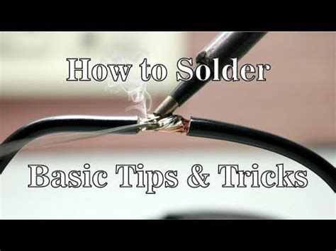
What is Solder Escape?
Solder escape, also known as solder wicking, is a common problem encountered during the soldering process. It occurs when molten solder flows away from the intended joint and spreads along the component leads or PCB traces. This unwanted flow of solder can cause short circuits, bridging between adjacent pins, and other issues that can compromise the integrity and functionality of the electronic assembly.
Causes of Solder Escape
Several factors can contribute to the occurrence of solder escape:
-
Excessive heat: Applying too much heat during soldering can cause the solder to become excessively fluid, increasing the likelihood of it flowing away from the joint.
-
Insufficient flux: Flux helps to clean the surfaces and promote proper solder flow. If there is not enough flux, or if the flux has become inactive, the solder may not flow properly and can escape from the joint.
-
Incorrect soldering technique: Poor soldering techniques, such as applying too much solder or not properly positioning the soldering iron, can lead to solder escape.
-
Contaminated surfaces: Dirty or oxidized component leads or PCB pads can hinder proper solder flow and cause the solder to wick away from the joint.
-
Inadequate pad design: If the PCB pads are too small or not properly designed, it can be difficult to contain the solder within the desired area.
Preventing Solder Escape
To minimize the occurrence of solder escape and ensure high-quality solder joints, follow these best practices:
1. Control Soldering Temperature
One of the key factors in preventing solder escape is maintaining the appropriate soldering temperature. The ideal temperature range for most soldering applications is between 315°C and 370°C (600°F to 700°F). Adjust your soldering iron’s temperature based on the type of solder and the size of the components being soldered.
| Solder Type | Temperature Range |
|---|---|
| Lead-based solder (Sn63/Pb37) | 315°C – 370°C (600°F – 700°F) |
| Lead-free solder (Sn96.5/Ag3.0/Cu0.5) | 370°C – 425°C (700°F – 800°F) |
2. Use Adequate Flux
Flux plays a crucial role in the soldering process by removing oxides, promoting solder flow, and ensuring proper wetting of the surfaces. When preventing solder escape, it is important to use an adequate amount of flux. Apply a thin layer of flux to the component leads and PCB pads before soldering. This will help the solder to flow evenly and stay within the intended area.
3. Employ Proper Soldering Technique
Proper soldering technique is essential for achieving reliable solder joints and preventing solder escape. Follow these guidelines:
- Use the appropriate soldering iron tip size for the component being soldered.
- Apply the soldering iron to both the component lead and the PCB pad simultaneously to heat them evenly.
- Feed the solder wire to the joint while maintaining contact with the soldering iron tip.
- Use just enough solder to create a concave fillet between the component lead and the PCB pad.
- Remove the soldering iron and allow the joint to cool without disturbance.
4. Ensure Clean Surfaces
Contaminated or oxidized surfaces can hinder proper solder flow and contribute to solder escape. Before soldering, make sure the component leads and PCB pads are clean and free from dirt, grease, or oxidation. Use a solvent cleaner or a gentle abrasive to remove any contaminants. Additionally, consider using a no-clean flux, which leaves minimal residue and reduces the need for post-soldering cleaning.
5. Optimize PCB Pad Design
Proper PCB pad design can help contain the solder within the desired area and prevent solder escape. Consider the following guidelines:
- Size the pads appropriately for the component leads. The pad should be slightly larger than the lead diameter to allow for proper solder fillets.
- Maintain adequate spacing between adjacent pads to prevent bridging.
- Use solder mask to define the solderable area and prevent solder from flowing beyond the pads.
- Consider using a solder mask defined (SMD) pad design, which provides better control over the solder flow compared to non-solder mask defined (NSMD) pads.

Solder Escape Remedies
Despite taking preventive measures, solder escape may still occur occasionally. If you encounter solder escape, here are some methods to remedy the situation:
-
Solder wick: Solder wick, also known as desoldering braid, is a copper braid that can be used to remove excess solder. Place the solder wick on the affected area and apply heat with the soldering iron. The excess solder will be drawn into the wick through capillary action.
-
Solder sucker: A solder sucker, or desoldering pump, is a vacuum-based tool that can be used to remove excess solder. Place the tip of the solder sucker near the excess solder and activate the pump to suck up the molten solder.
-
Flux and re-soldering: If the solder has escaped but not caused any shorts or bridging, you can try applying additional flux and re-soldering the joint. The flux will help the solder to flow back to the intended area.
-
Mechanical removal: In some cases, you may need to remove the excess solder mechanically using tweezers, a knife, or a scalpel. Be cautious not to damage the components or PCB traces in the process.

FAQ
-
Q: What is the main cause of solder escape?
A: The main cause of solder escape is excessive heat during the soldering process, which makes the solder too fluid and allows it to flow away from the intended joint. -
Q: Can insufficient flux lead to solder escape?
A: Yes, insufficient flux can contribute to solder escape. Flux helps to clean the surfaces and promote proper solder flow. If there is not enough flux, the solder may not flow properly and can escape from the joint. -
Q: What is the ideal temperature range for soldering?
A: The ideal temperature range for most soldering applications is between 315°C and 370°C (600°F to 700°F) for lead-based solder and between 370°C and 425°C (700°F to 800°F) for lead-free solder. -
Q: How can I remove excess solder caused by solder escape?
A: You can remove excess solder using tools such as solder wick (desoldering braid), a solder sucker (desoldering pump), or by mechanically removing it with tweezers or a knife. In some cases, applying additional flux and re-soldering the joint may also help. -
Q: What role does PCB pad design play in preventing solder escape?
A: Proper PCB pad design can help contain the solder within the desired area and prevent solder escape. This includes sizing the pads appropriately for the component leads, maintaining adequate spacing between adjacent pads, using solder mask to define the solderable area, and considering solder mask defined (SMD) pad designs.
By understanding the causes of solder escape and implementing preventive measures such as controlling soldering temperature, using adequate flux, employing proper soldering techniques, ensuring clean surfaces, and optimizing PCB pad design, you can significantly reduce the occurrence of solder escape and achieve reliable solder joints in your electronic assemblies.

No responses yet