What is PCB Galvanization?
PCB galvanization, also known as PCB plating, is a metal finishing process that deposits a thin layer of metal, usually zinc, onto the copper surfaces of a printed circuit board. This protective layer acts as a barrier against environmental factors that can cause the copper to deteriorate over time, such as moisture, air, and chemical exposure.
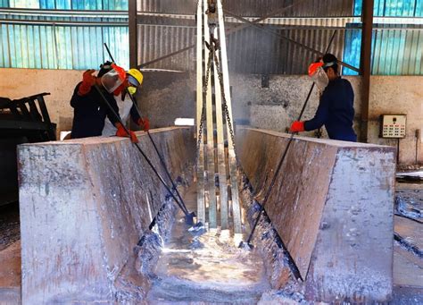
The galvanization process involves submerging the PCB into an electrolyte solution containing dissolved metal ions. By applying an electric current, the metal ions are attracted to the copper surfaces of the PCB, forming a uniform coating. The thickness of the galvanized layer can be precisely controlled by adjusting the current and duration of the electroplating process.
Benefits of Galvanising PCBs
Galvanising PCBs offers several key benefits that enhance the overall quality and reliability of the finished product:
1. Corrosion resistance
The primary benefit of galvanizing PCBs is the significant improvement in corrosion resistance. The zinc coating acts as a sacrificial layer, preferentially corroding instead of the underlying copper. This sacrificial protection prolongs the life of the PCB by preventing the formation of copper oxide, which can lead to reduced conductivity and potential circuit failures.
2. Improved solderability
Galvanized surfaces also provide better solderability compared to bare copper. The zinc layer helps prevent the formation of surface oxides that can hinder the wetting of solder during the assembly process. This results in stronger, more reliable solder joints and reduces the likelihood of defects such as cold joints or poor wetting.
3. Enhanced mechanical properties
The galvanizing process can also improve the mechanical properties of the PCB. The added metal layer increases the thickness and rigidity of the copper traces, making them more resistant to physical damage, such as scratches or impacts. This is particularly beneficial for PCBs that are subject to mechanical stresses during assembly or in their end-use applications.
4. Compatibility with various surface finishes
Galvanised PCBs are compatible with a wide range of surface finishes commonly used in the electronics industry. The zinc layer provides an excellent base for applying additional finishes, such as HASL (Hot Air Solder Leveling), ENIG (Electroless Nickel Immersion Gold), or OSP (Organic Solderability Preservative). These finishes can further enhance the solderability, corrosion resistance, and aesthetic appearance of the PCB.

The PCB Galvanization Process
The PCB galvanization process involves several key steps to ensure a high-quality, uniform coating:
1. Cleaning
Before galvanizing, the PCB must be thoroughly cleaned to remove any contaminants, such as dirt, grease, or oxides, from the copper surfaces. This is typically done using a series of chemical baths, including alkaline cleaners, acid cleaners, and micro-etches. Proper cleaning ensures good adhesion of the galvanized layer to the copper substrate.
2. Activation
After cleaning, the PCB undergoes an activation step to further improve the adhesion of the galvanized layer. This usually involves dipping the PCB in an acidic solution, such as dilute sulfuric acid, which etches the copper surface and creates a micro-roughened profile. The increased surface area and roughness promote better mechanical interlocking between the copper and the deposited metal.
3. Electroplating
The actual galvanization takes place in an electroplating bath containing a solution of dissolved metal salts, typically zinc sulfate or zinc chloride. The PCB is connected to the negative terminal (cathode) of a power supply, while a zinc anode is connected to the positive terminal. When an electric current is applied, the positively-charged zinc ions are attracted to the negatively-charged PCB, forming a uniform layer of zinc on the exposed copper surfaces.
The thickness of the galvanized layer can be controlled by adjusting the current density and plating time. Typical zinc layer thicknesses range from 5 to 15 microns, depending on the specific requirements of the PCB application.
4. Rinsing and drying
After electroplating, the PCB is rinsed in deionized water to remove any residual plating solution. It is then dried using hot air or infrared lamps to prevent water spots or stains from forming on the surface.
5. Inspection and quality control
The galvanized PCB undergoes a thorough visual inspection to ensure uniform coverage, absence of defects (such as pits, nodules, or blisters), and proper adhesion of the zinc layer. Additional quality control measures may include cross-sectional analysis, thickness measurements, and adhesion tests to verify that the galvanized coating meets the specified requirements.

Key Considerations for PCB Galvanization
When galvanizing PCBs, several key factors must be considered to ensure optimal results:
1. Copper thickness and trace width
The thickness of the copper traces and pads on the PCB can affect the uniformity and adhesion of the galvanized layer. Thicker copper may require longer plating times or higher current densities to achieve the desired zinc thickness. Additionally, very fine trace widths or spacing may be more challenging to galvanize uniformly, as the high current density in these areas can lead to uneven deposition or burning of the resist.
2. Masking and resist compatibility
During the galvanization process, areas of the PCB that should not be plated, such as through-holes, connectors, or test points, must be protected using a plating resist. The resist material must be compatible with the galvanizing process and able to withstand the chemical baths and electric currents involved. Proper masking ensures that only the desired areas of the PCB are galvanized, maintaining the functionality and reliability of the circuit.
3. Hydrogen embrittlement
In some cases, the galvanizing process can lead to hydrogen embrittlement of the PCB substrate, particularly in high-strength, low-alloy steels. Hydrogen embrittlement occurs when hydrogen atoms diffuse into the metal lattice during electroplating, causing a reduction in ductility and an increased risk of brittle fracture. To mitigate this issue, careful control of the plating parameters, such as current density and pH, is necessary. Post-plating baking can also help to drive out any absorbed hydrogen.
4. Environmental considerations
Galvanization processes generate waste streams that contain heavy metals and other pollutants. Proper treatment and disposal of these wastes are critical to minimizing the environmental impact of PCB manufacturing. This includes the use of closed-loop systems, waste reduction strategies, and adherence to local and international environmental regulations.

Alternative PCB Surface Finishes
While galvanizing is a popular choice for PCB surface finishing, there are several other options available that offer unique benefits and characteristics:
1. HASL (Hot Air Solder Leveling)
HASL is a widely used surface finish that involves dipping the PCB in molten solder and then using hot air to level the solder on the surface. HASL provides excellent solderability and is relatively inexpensive. However, it can result in an uneven surface finish and may not be suitable for fine-pitch components.
2. ENIG (Electroless Nickel Immersion Gold)
ENIG is a two-layer surface finish that consists of a layer of electroless nickel followed by a thin layer of immersion gold. ENIG offers excellent flatness, solderability, and shelf life, making it a popular choice for high-density, fine-pitch PCBs. However, it is more expensive than other finishes and can be prone to “black pad” issues if not processed correctly.
3. OSP (Organic Solderability Preservative)
OSP is a thin, organic coating that is applied to the copper surfaces of the PCB to prevent oxidation and maintain solderability. OSP is a cost-effective and environmentally friendly option, as it does not contain any heavy metals. However, it has a limited shelf life and may not provide the same level of protection as metallic finishes.
4. Immersion Silver
Immersion silver is a thin, metallic coating that provides good solderability and conductivity. It is a lead-free, RoHS-compliant finish that is less expensive than ENIG. However, immersion silver can tarnish over time and may not be suitable for applications with strict aesthetic requirements.
The choice of surface finish depends on various factors, such as the intended application, component types, environmental requirements, and cost constraints. The following table compares the key characteristics of these surface finishes:
| Finish | Solderability | Durability | Flatness | Cost |
|---|---|---|---|---|
| Galvanized | Good | Excellent | Good | Moderate |
| HASL | Excellent | Good | Poor | Low |
| ENIG | Excellent | Excellent | Excellent | High |
| OSP | Good | Poor | Excellent | Low |
| Immersion Silver | Good | Moderate | Excellent | Moderate |
FAQ
1. How long does the galvanizing process take for a typical PCB?
The duration of the galvanizing process depends on the desired thickness of the zinc layer and the size of the PCB. For a standard thickness of 5-15 microns, the electroplating process typically takes 15-30 minutes. However, the entire process, including cleaning, activation, and drying, can take several hours.
2. Can all types of PCBs be galvanized?
Most PCBs can be galvanized, including rigid, flexible, and rigid-flex boards. However, some special materials or very fine features may require adjustments to the galvanizing process parameters or may not be suitable for galvanization at all. It is essential to consult with your PCB manufacturer to determine the feasibility of galvanizing your specific PCB design.
3. How does the cost of galvanizing compare to other surface finishes?
Galvanizing is generally more expensive than OSP and HASL but less expensive than ENIG and immersion silver. The exact cost will depend on factors such as the size of the PCB, the thickness of the galvanized layer, and the volume of production. In general, galvanizing offers a good balance of cost and performance for many applications.
4. Can galvanized PCBs be reworked or repaired?
Yes, galvanized PCBs can be reworked or repaired, but it may be more challenging than with other surface finishes. The zinc layer must be removed from the area to be reworked, typically using abrasive methods or chemical etching. After the repair is complete, the area can be re-galvanized or protected using alternative coatings, such as conductive epoxy or solder mask.
5. What are the main challenges associated with PCB galvanization?
Some of the main challenges in PCB galvanization include achieving uniform zinc deposition on complex board geometries, maintaining compatibility with fine-pitch components and high-density designs, and minimizing the environmental impact of the galvanizing process. Proper process control, equipment maintenance, and adherence to best practices can help mitigate these challenges and ensure high-quality results.
Conclusion
Galvanising PCBs is a highly effective method for enhancing the durability, solderability, and overall reliability of printed circuit boards. By applying a protective layer of zinc to the copper surfaces, galvanizing helps prevent corrosion, oxidation, and mechanical damage, extending the lifespan of the PCB.
The galvanization process involves a series of steps, including cleaning, activation, electroplating, and quality control, to ensure a uniform, adherent coating. Key considerations for successful galvanization include copper thickness, masking and resist compatibility, hydrogen embrittlement, and environmental impact.
While galvanizing is a popular choice, alternative surface finishes such as HASL, ENIG, OSP, and immersion silver offer unique benefits and may be more suitable for certain applications. The choice of surface finish depends on factors such as cost, performance requirements, and manufacturing capabilities.
As PCB technology continues to advance, with increasing complexity and miniaturization, the importance of effective surface finishing methods like galvanization will only grow. By understanding the principles, processes, and challenges associated with PCB galvanization, manufacturers can make informed decisions and produce high-quality, reliable PCBs that meet the demanding requirements of modern electronics applications.
No responses yet