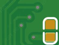
What are Vias in PCBs?
Vias are small holes drilled through a PCB that allow electrical connections between different layers of the board. They are essential for creating multi-layer PCBs and enabling complex circuitry designs. There are several types of vias used in PCBs:
| Via Type | Description |
|---|---|
| Through Hole Via | Drilled through the entire board, connecting all layers |
| Blind Via | Connects an outer layer to an inner layer, but not all the way through |
| Buried Via | Connects inner layers without reaching the outer layers |
| Microvia | A small via (typically less than 0.15mm in diameter) used for high-density designs |
Why is Via covering Necessary?
Via covering serves several important purposes in PCB manufacturing:
- Preventing Solder Wicking: During the soldering process, molten solder can flow into the vias, causing a phenomenon known as solder wicking. This can lead to insufficient solder on the component pads, resulting in poor connections and potential reliability issues. By covering the vias, the soldermask prevents solder from entering the holes.
- Protecting Against Contaminants: Exposed vias can act as entry points for contaminants, such as dust, dirt, and moisture, which can cause short circuits, corrosion, and other issues that affect the performance and longevity of the PCB. Via covering seals the holes, preventing contaminants from entering the board.
- Improving Insulation: Covering the vias with a soldermask enhances the insulation between the different layers of the PCB, reducing the risk of electrical shorts and improving the overall reliability of the board.
- Enhancing Aesthetics: Exposed vias can detract from the visual appeal of a PCB. By covering them with a soldermask, the board looks cleaner and more professional.
Via Covering Materials
Several materials can be used for via covering, each with its own advantages and disadvantages:
Soldermask
Soldermask, also known as solder resist, is the most common material used for via covering. It is a thin, protective layer applied to the surface of the PCB, typically made from a photoimageable polymer. Soldermask is available in various colors, with green being the most popular.
Advantages of using soldermask for via covering:
– Excellent insulation properties
– Protects against solder wicking and contaminants
– Enhances the visual appearance of the PCB
– Cost-effective and widely available
Disadvantages of soldermask:
– May not provide complete coverage for small or high-aspect-ratio vias
– Can be prone to cracking or peeling if not applied properly
Epoxy
Epoxy is another material that can be used for via covering. It is a two-part resin that hardens when mixed, forming a strong, durable covering over the vias.
Advantages of using epoxy for via covering:
– Provides excellent coverage, even for small or high-aspect-ratio vias
– Offers superior mechanical strength and durability
– Can be used for selective via covering
Disadvantages of epoxy:
– More expensive than soldermask
– Requires additional processing steps
– Can be difficult to remove if rework is necessary
Conductive Ink
Conductive ink is a specialized material that can be used for via covering in certain applications. It is a printable ink that contains conductive particles, such as silver or copper, which allow electrical signals to pass through the covered via.
Advantages of using conductive ink for via covering:
– Enables electrical connections through the covered via
– Can be used for creating shielded vias or providing EMI protection
– Allows for more Flexible Circuit Designs
Disadvantages of conductive ink:
– Significantly more expensive than soldermask or epoxy
– Requires specialized equipment for application
– May not provide the same level of insulation as non-conductive materials

Via Covering Techniques
There are several techniques used for applying via covering materials to PCBs:
Screen Printing
Screen printing is the most common method for applying soldermask to PCBs, including via covering. The process involves using a fine mesh screen to transfer the soldermask onto the board, covering the vias and other areas that need protection.
Advantages of screen printing:
– Fast and cost-effective for high-volume production
– Provides consistent coverage and thickness
– Can be used with a variety of soldermask materials
Disadvantages of screen printing:
– May not provide complete coverage for small or high-aspect-ratio vias
– Requires the creation of screens for each unique PCB design
Liquid Photoimageable Soldermask (LPISM)
LPISM is a photoimageable soldermask that is applied to the PCB as a liquid and then exposed to UV light through a photomask. The exposed areas harden, while the unexposed areas are washed away, leaving a precise pattern of soldermask on the board.
Advantages of LPISM:
– Provides high-resolution coverage, suitable for small vias and fine features
– Allows for the creation of complex soldermask patterns
– Can be applied in a thin, even layer
Disadvantages of LPISM:
– More expensive than screen printing
– Requires specialized equipment and processing steps
– May have a longer lead time due to the additional processing required
Dry Film Soldermask (DFSM)
DFSM is a photoimageable soldermask that comes in the form of a dry film. The film is laminated onto the PCB, exposed to UV light through a photomask, and then developed, leaving a pattern of soldermask on the board.
Advantages of DFSM:
– Provides consistent thickness and coverage
– Suitable for covering small vias and fine features
– Can be applied quickly and easily
Disadvantages of DFSM:
– More expensive than screen printing
– May not conform well to uneven board surfaces
– Can be prone to air bubbles or wrinkles if not applied properly

Design Considerations for Via Covering
When designing a PCB that will use via covering, there are several factors to consider:
- Via Size and Aspect Ratio: The size and aspect ratio of the vias can affect the ability of the covering material to provide complete coverage. Smaller vias and those with high aspect ratios (depth to diameter) may be more challenging to cover effectively.
- Via Location: The location of the vias on the PCB can impact the effectiveness of the via covering process. Vias located close to the edge of the board or in areas with high component density may be more difficult to cover completely.
- Soldermask Clearance: When using soldermask for via covering, it is essential to provide adequate clearance around the vias to ensure proper adhesion and coverage. The clearance should be specified in the PCB design files and communicated to the manufacturer.
- Material Compatibility: The choice of via covering material should be compatible with the PCB substrate, soldermask, and other materials used in the manufacturing process. Incompatible materials can lead to adhesion issues, delamination, or other problems that affect the reliability of the board.
- Electrical Requirements: If the vias need to be electrically connected, as in the case of shielded vias or those used for EMI protection, the choice of via covering material should take into account the electrical properties required for the application.
FAQ
- Q: What is the difference between via tenting and Via Filling?
A: Via tenting involves covering the via with a soldermask or other material on the surface of the PCB, while via filling involves filling the entire via with a material, such as epoxy or conductive ink. - Q: Can via covering be used on both sides of the PCB?
A: Yes, via covering can be applied to both sides of the PCB, depending on the design requirements and the manufacturing process used. - Q: Is via covering necessary for all PCBs?
A: No, via covering is not always necessary. The decision to use via covering depends on the specific requirements of the PCB, such as the operating environment, the complexity of the circuit, and the reliability needs of the application. - Q: Can via covering be selectively applied to specific vias on a PCB?
A: Yes, selective via covering is possible using materials like epoxy or conductive ink, which can be applied to individual vias as needed. - Q: How does via covering affect the cost of PCB manufacturing?
A: Via covering generally adds to the cost of PCB manufacturing, as it requires additional materials and processing steps. The cost impact depends on the specific via covering method and material used, as well as the volume of the production run.
In conclusion, via covering is an essential process in PCB manufacturing that helps ensure the reliability, durability, and functionality of the board. By understanding the various materials, techniques, and design considerations involved in via covering, PCB designers and manufacturers can make informed decisions to create high-quality, reliable products that meet the needs of their applications.
No responses yet