Introduction to Solder Stencils
Solder stencils are an essential tool in the world of electronics manufacturing. They are thin sheets of metal, typically stainless steel, with laser-cut openings that correspond to the pads on a printed circuit board (PCB). These stencils are used to apply solder paste to the PCB, ensuring precise and uniform placement of the paste, which is crucial for the successful assembly of surface-mount components.
What are Solder Stencils?
Solder stencils are a key component in the surface-mount technology (SMT) assembly process. They are designed to match the layout of the PCB, with openings that align with the pads where components will be placed. The stencil is placed over the PCB, and solder paste is applied using a squeegee or automated stencil printer. The paste is forced through the openings, depositing a precise amount onto each pad.
Benefits of Using Solder Stencils
Using solder stencils offers several advantages in the PCB Assembly process:
- Precision: Solder stencils ensure accurate and consistent placement of solder paste on the PCB pads, reducing the risk of bridging or insufficient solder.
- Efficiency: Stencils allow for the rapid application of solder paste to multiple PCBs, streamlining the assembly process.
- Repeatability: Stencils provide consistent results, ensuring that each PCB receives the same amount of solder paste in the same locations.
- Cost-effective: Using solder stencils reduces the amount of solder paste waste and minimizes the need for rework, ultimately saving time and money.
Types of Solder Stencils
There are several types of solder stencils available, each with its own unique characteristics and applications.
Stainless Steel Stencils
Stainless steel stencils are the most common type used in the electronics industry. They are durable, long-lasting, and offer excellent paste release properties. These stencils are typically laser-cut to ensure precise openings and can be used for a wide range of PCB designs.
Polyimide Stencils
Polyimide stencils, also known as kapton stencils, are made from a flexible, high-temperature resistant plastic material. They are often used for prototyping or low-volume production runs, as they are less durable than stainless steel stencils but offer a more cost-effective solution for smaller projects.
Nickel Stencils
Nickel stencils are known for their exceptional durability and long lifespan. They are more expensive than stainless steel stencils but are ideal for high-volume production or applications that require a high level of abrasion resistance.
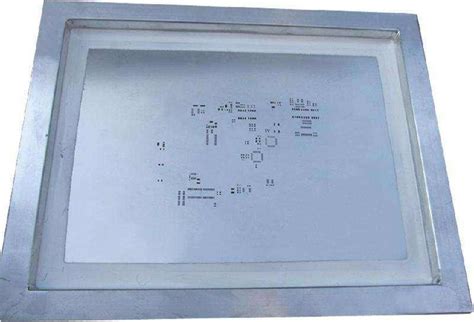
Framed Stencils
Framed stencils are mounted in a rigid frame, which helps to maintain the stencil’s flatness and prevents warping. This is particularly important for larger PCBs or designs with fine-pitch components, where even slight distortions can lead to assembly issues.
Frameless Stencils
Frameless stencils are not mounted in a frame and are typically used for smaller PCBs or in situations where the stencil needs to be frequently changed. They are more flexible and easier to store than framed stencils but may be more prone to warping or damage if not handled carefully.

Designing Solder Stencils
Designing a solder stencil involves several key considerations to ensure optimal performance and results.
Aperture Design
Aperture design refers to the size, shape, and layout of the openings in the stencil. The apertures must be carefully designed to match the pads on the PCB and to accommodate the specific requirements of the solder paste and components being used.
Aperture Size
The size of the apertures is typically determined by the size of the pads on the PCB, the type of solder paste being used, and the desired amount of paste deposition. As a general rule, the aperture should be slightly larger than the pad to allow for proper paste release and to account for any slight misalignment during the stencil printing process.
| Pad Size (mm) | Aperture Size (mm) |
|---|---|
| 0.5 x 0.5 | 0.6 x 0.6 |
| 0.8 x 0.8 | 0.9 x 0.9 |
| 1.0 x 1.0 | 1.1 x 1.1 |
Aperture Shape
The shape of the apertures can also impact the solder paste deposition and the final solder joint quality. Common aperture shapes include:
- Square: The most common shape, suitable for most SMD pads.
- Rectangular: Used for oblong or rectangular pads, such as those found on chip resistors or capacitors.
- Circular: Used for round pads, such as those found on ball grid array (BGA) packages.
- D-shaped: Used for pads with one rounded end, such as those found on some connectors.
Aperture Orientation
The orientation of the apertures should match the orientation of the pads on the PCB. This is particularly important for components with polarized or directional pads, such as diodes or electrolytic capacitors.
Stencil Thickness
The thickness of the solder stencil determines the amount of solder paste deposited on the pads. Thicker stencils deposit more paste, while thinner stencils deposit less. The optimal stencil thickness depends on several factors, including the size and pitch of the components, the solder paste type, and the desired solder joint profile.
| Pitch (mm) | Stencil Thickness (mm) |
|---|---|
| 0.5 | 0.100 – 0.125 |
| 0.65 | 0.125 – 0.150 |
| 0.8 | 0.150 – 0.200 |
| 1.0 | 0.200 – 0.250 |
Fiducial Marks
Fiducial marks are reference points on the stencil that are used to align the stencil with the PCB during the printing process. These marks should be clearly visible and positioned in the same locations on both the stencil and the PCB. Typically, at least three fiducial marks are used to ensure proper alignment in both the X and Y axes, as well as rotational alignment.

Solder Paste Selection
Selecting the appropriate solder paste is crucial for achieving high-quality solder joints and reliable PCB assembly.
Solder Paste Composition
Solder paste is a mixture of tiny solder spheres (typically tin, lead, and silver) suspended in a flux medium. The composition of the solder paste determines its melting temperature, wetting properties, and final solder joint strength.
Common solder paste alloys include:
- Tin-Lead (Sn63/Pb37): Traditional leaded solder, with a melting point of 183°C.
- Tin-Silver-Copper (SAC305): Lead-free solder, with a melting point of 217-220°C.
- Tin-Bismuth (Sn42/Bi57.6): Low-temperature lead-free solder, with a melting point of 138°C.
Solder Paste Particle Size
The particle size of the solder spheres in the paste affects the printability and the final solder joint quality. Smaller particle sizes allow for finer pitch components and more precise paste deposition, but may be more prone to clogging the stencil apertures.
| Type | Particle Size (μm) |
|---|---|
| Type 1 | 150-75 |
| Type 2 | 75-45 |
| Type 3 | 45-25 |
| Type 4 | 38-20 |
| Type 5 | 30-15 |
| Type 6 | 15-5 |
Solder Paste Flux
The flux in the solder paste serves to remove oxides from the metal surfaces, promote wetting, and protect the solder joint from oxidation during the reflow process. There are several types of flux, each with different activity levels and residue characteristics.
- Rosin (R): Mildly active, leaves a non-conductive residue.
- Rosin Mildly Activated (RMA): Moderately active, leaves a non-conductive residue.
- Water-Soluble (WS): Highly active, leaves a conductive residue that must be cleaned.
- No-Clean (NC): Low activity, leaves a minimal, non-conductive residue that does not require cleaning.

Solder Stencil Printing Process
The solder stencil printing process involves several key steps to ensure accurate and consistent solder paste deposition.
Stencil Alignment
The first step in the printing process is to align the stencil with the PCB. This is typically done using the fiducial marks on the stencil and PCB, either manually or with the aid of an automated vision system. Proper alignment is crucial to ensure that the solder paste is deposited in the correct locations on the pads.
Solder Paste Application
Once the stencil is aligned, the solder paste is applied to the top surface of the stencil. This can be done manually using a squeegee or automatically using a stencil printer. The paste is then spread across the stencil, forcing it through the apertures and onto the PCB pads.
Manual Solder Paste Application
For manual solder paste application, a metal or plastic squeegee is used to spread the paste across the stencil. The squeegee should be held at a 45-60° angle to the stencil and moved in a smooth, consistent motion to ensure even paste distribution. Excessive pressure or speed can lead to paste bleeding or inconsistent deposition.
Automatic Solder Paste Application
Automatic sencil printers use a motorized squeegee system to apply the solder paste. These machines offer more consistent results and higher throughput than manual methods, making them ideal for high-volume production. Key parameters to consider when setting up an automatic stencil printer include:
- Squeegee pressure
- Squeegee speed
- Separation speed (the speed at which the stencil is lifted from the PCB)
- Print gap (the distance between the stencil and PCB during printing)
Stencil Cleaning
After the solder paste has been applied, the stencil must be cleaned to remove any excess paste or residue. This is important to prevent paste buildup, which can lead to aperture clogging and inconsistent printing results. Stencils can be cleaned manually using solvents and wipes or automatically using a stencil cleaning machine.
Under-stencil Cleaning
Under-stencil cleaning is a technique used to remove solder paste residue from the bottom side of the stencil. This is typically done using a specialized cleaning sheet or roll that is placed between the stencil and PCB during the printing process. As the squeegee moves across the stencil, the cleaning material removes any excess paste, helping to maintain print quality and extend the life of the stencil.
Solder Stencil Maintenance
Proper maintenance of solder stencils is essential for ensuring consistent, high-quality printing results and extending the life of the stencils.
Stencil Inspection
Regular inspection of the solder stencil is important to identify any damage, wear, or paste buildup that could affect print quality. This can be done visually or using specialized inspection equipment, such as a stencil microscope or 3D solder paste inspection system.
Key areas to inspect include:
- Aperture edges: Look for any signs of wear, damage, or rounding that could affect paste release.
- Stencil surface: Check for any scratches, dents, or other damage that could impact print quality.
- Aperture walls: Inspect for any paste buildup or clogging that could restrict paste flow.
Stencil Cleaning
Regular cleaning of the solder stencil is crucial for maintaining print quality and preventing paste buildup. Stencils should be cleaned after every print cycle or as needed based on the specific manufacturing process and solder paste type.
Cleaning methods include:
- Manual cleaning: Using solvents and wipes to manually remove paste residue.
- Ultrasonic cleaning: Immersing the stencil in an Ultrasonic Cleaner with a suitable solvent to remove stubborn residue.
- Automatic cleaning: Using a stencil cleaning machine to automatically clean the stencil with solvents and brushes.
Stencil Storage
Proper storage of solder stencils is important to prevent damage and maintain their performance. Stencils should be stored in a clean, dry environment, away from any sources of moisture, dust, or debris. They should be placed in protective packaging, such as a stencil tray or folder, to prevent scratches or dents during handling and storage.
When storing framed stencils, it is important to ensure that the frames are not subjected to excessive pressure or weight, as this can cause warping or damage to the stencil. Frameless stencils should be stored flat to prevent any distortion or creasing.
Troubleshooting Common Solder Stencil Issues
Even with proper design, selection, and maintenance, solder stencil issues can arise during the printing process. Here are some common problems and their potential solutions:
Insufficient Solder Paste Deposition
If the solder paste deposition is too low, it can lead to weak or incomplete solder joints. Possible causes and solutions include:
- Causes:
- Clogged stencil apertures
- Low solder paste viscosity
- Incorrect stencil thickness
- Insufficient squeegee pressure
- Solutions:
- Clean the stencil to remove any blockages
- Use a thicker solder paste or adjust the print parameters
- Increase the stencil thickness
- Increase the squeegee pressure
Excessive Solder Paste Deposition
Excessive solder paste deposition can lead to bridging, solder balls, or other defects. Possible causes and solutions include:
- Causes:
- Worn or damaged stencil apertures
- High solder paste viscosity
- Excessive stencil thickness
- Excessive squeegee pressure
- Solutions:
- Replace or repair the damaged stencil
- Use a thinner solder paste or adjust the print parameters
- Decrease the stencil thickness
- Reduce the squeegee pressure
Solder Paste Smearing
Solder paste smearing occurs when the paste is dragged across the PCB surface, leading to poor print definition and potential defects. Possible causes and solutions include:
- Causes:
- Poor stencil-to-PCB gasketing
- Excessive squeegee pressure
- Slow print speed
- Incorrect squeegee angle
- Solutions:
- Ensure proper stencil alignment and gasketing
- Reduce the squeegee pressure
- Increase the print speed
- Adjust the squeegee angle to 45-60°
Stencil Warping
Warped stencils can lead to uneven solder paste deposition and poor print quality. Possible causes and solutions include:
- Causes:
- Improper storage or handling
- Excessive cleaning or exposure to solvents
- Uneven frame mounting
- Thermal expansion during printing
- Solutions:
- Store stencils properly in protective packaging
- Use appropriate cleaning methods and solvents
- Ensure even frame mounting and tension
- Allow stencils to acclimate to the printing environment
Conclusion
Solder stencils play a critical role in the surface-mount assembly process, ensuring accurate and consistent solder paste deposition for high-quality PCB assembly. By understanding the types of stencils available, design considerations, solder paste selection, printing process, maintenance requirements, and common troubleshooting techniques, manufacturers can optimize their solder stencil performance and achieve reliable, defect-free PCB assemblies.
As the electronics industry continues to evolve, with smaller components and more complex designs, the importance of effective solder stencil solutions will only continue to grow. By staying up-to-date with the latest technologies, best practices, and troubleshooting methods, manufacturers can ensure that their solder stencil processes remain efficient, reliable, and cost-effective.
Frequently Asked Questions (FAQ)
- What is the difference between a solder stencil and a solder screen?
-
A solder stencil is a thin, laser-cut metal sheet with apertures that match the PCB pads, while a solder screen is a woven wire mesh with a photoimaged emulsion defining the apertures. Stencils are more commonly used in modern SMT assembly due to their superior print definition and durability.
-
How often should I clean my solder stencil?
- Solder stencils should be cleaned after every print cycle or as needed based on the specific manufacturing process and solder paste type. Regular cleaning helps maintain print quality, prevent paste buildup, and extend the life of
No responses yet