Introduction to PCB Copper Layers
Printed Circuit Boards (PCBs) are the backbone of modern electronics. They provide a platform for electronic components to be mounted and interconnected, enabling the creation of complex electronic circuits. One of the critical elements of a PCB is the copper layer. In this article, we will explore what PCB copper layers are, their types, manufacturing process, and their importance in PCB design and functionality.
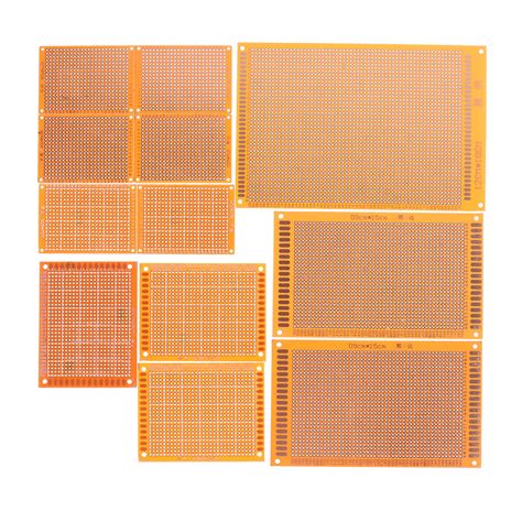
What are PCB Copper Layers?
PCB copper layers are thin sheets of copper foil laminated onto a non-conductive substrate, typically made of fiberglass or other composite materials. These copper layers are used to create the conductive pathways that allow electrical signals to flow between components on the PCB. The number of copper layers in a PCB can vary depending on the complexity of the circuit and the desired functionality.
Types of PCB Copper Layers
There are several types of PCB copper layers, each with its own characteristics and applications. The most common types include:
-
Single-sided PCBs: These PCBs have copper on only one side of the substrate. They are the simplest and most cost-effective type of PCB, suitable for basic electronic circuits.
-
Double-sided PCBs: These PCBs have copper layers on both sides of the substrate, allowing for more complex circuits and higher component density. The two copper layers are connected using through-hole vias.
-
Multi-layer PCBs: These PCBs have three or more copper layers, with insulating layers separating them. Multi-layer PCBs enable even more complex circuits and higher component density, as well as improved signal integrity and electromagnetic interference (EMI) reduction.
-
Flexible PCBs: These PCBs use flexible substrates, such as polyimide, with copper layers laminated on top. Flexible PCBs are used in applications where the circuit needs to bend or flex, such as in wearable electronics or mobile devices.
-
Rigid-Flex PCBs: These PCBs combine rigid and flexible sections, allowing for the benefits of both types of PCBs in a single design. Rigid-flex PCBs are often used in aerospace, military, and medical applications.
PCB Copper Layer Manufacturing Process
The manufacturing process for PCB copper layers involves several steps, each of which is critical to ensuring the quality and reliability of the final product. The main steps in the process are:
-
Substrate Preparation: The non-conductive substrate, such as FR-4 fiberglass, is cut to the desired size and shape. The substrate is then cleaned and inspected for any defects.
-
Copper Foil Lamination: A thin sheet of copper foil is laminated onto the substrate using heat and pressure. The copper foil is typically pre-treated with a surface finish to improve adhesion and prevent oxidation.
-
Photoresist Application: A light-sensitive photoresist is applied to the copper layer. This photoresist will be used to create the desired circuit pattern.
-
Exposure and Development: The photoresist-coated copper layer is exposed to UV light through a photomask, which contains the circuit pattern. The exposed photoresist is then developed, leaving the desired pattern on the copper layer.
-
Etching: The unwanted copper is removed using a chemical etching process, leaving only the desired circuit pattern on the substrate.
-
Inspection and Testing: The PCB is inspected for any defects or inconsistencies, and electrical tests are performed to ensure proper functionality.
-
Surface Finishing: A surface finish, such as solder mask or silkscreen, is applied to protect the copper layers and improve solderability.

Importance of PCB Copper Layers in PCB Design and Functionality
PCB copper layers play a crucial role in the design and functionality of electronic circuits. Some of the key benefits and considerations related to PCB copper layers include:
-
Signal Integrity: Proper design and layout of PCB copper layers can help maintain signal integrity by minimizing crosstalk, reflections, and other signal distortions. This is particularly important in high-speed and high-frequency applications.
-
Power Distribution: PCB copper layers are used to distribute power to the various components on the board. Adequate copper thickness and proper layout techniques are essential to ensure reliable power delivery and minimize voltage drop.
-
Electromagnetic Compatibility (EMC): Careful design of PCB copper layers can help reduce electromagnetic interference (EMI) and improve electromagnetic compatibility (EMC). Techniques such as proper grounding, shielding, and the use of ground planes can help mitigate EMI issues.
-
Thermal Management: Copper layers can also help dissipate heat generated by components on the PCB. Proper thermal management is essential to ensure the long-term reliability and performance of the electronic circuit.
-
Manufacturing Considerations: The choice of PCB copper layer type and thickness can impact the manufacturing process and cost. For example, thicker copper layers may require longer etching times and may be more expensive, while thinner layers may be more prone to manufacturing defects.

PCB Copper Layer Thickness and Weight
The thickness and weight of PCB copper layers are important factors to consider in PCB design. Copper thickness is typically measured in ounces per square foot (oz/ft²) or microns (µm). The most common copper thicknesses used in PCBs are:
| Copper Thickness (oz/ft²) | Copper Thickness (µm) |
|---|---|
| 0.5 oz/ft² | 17 µm |
| 1 oz/ft² | 35 µm |
| 2 oz/ft² | 70 µm |
| 3 oz/ft² | 105 µm |
| 4 oz/ft² | 140 µm |
The choice of copper thickness depends on several factors, such as the current carrying requirements, the desired impedance, and the manufacturing capabilities. Thicker copper layers can carry more current and provide better thermal dissipation, but they may be more expensive and harder to manufacture.
Copper weight, on the other hand, refers to the total amount of copper used in the PCB, taking into account the number of layers and their respective thicknesses. Copper weight is often expressed in grams per square meter (g/m²) or pounds per square foot (lb/ft²).

Advanced Topics in PCB Copper Layers
High-Frequency PCB Design Considerations
In high-frequency applications, such as radio frequency (RF) and microwave circuits, the design of PCB copper layers becomes even more critical. Some key considerations for high-frequency PCB design include:
-
Controlled Impedance: Maintaining a consistent and controlled impedance throughout the signal path is essential to minimize reflections and signal distortions. This is achieved through careful design of the copper trace width, thickness, and spacing, as well as the use of specialized materials and layup techniques.
-
Skin Effect: At high frequencies, current tends to flow along the surface of the conductor, a phenomenon known as skin effect. This can lead to increased losses and signal attenuation. To mitigate skin effect, designers may use thinner copper layers or specialized surface finishes, such as silver or gold plating.
-
Dielectric Materials: The choice of dielectric material becomes crucial in high-frequency PCBs, as the material properties, such as dielectric constant and loss tangent, can significantly impact signal propagation and loss. Low-loss materials, such as PTFE (Teflon) or Rogers laminates, are often used in high-frequency applications.
Copper Plating in PCBs
In addition to laminated copper layers, PCBs may also utilize copper plating for various purposes, such as:
-
Through-hole Plating: Copper is plated inside the drilled holes of a PCB to create electrical connections between layers. This process is known as through-hole plating and is essential for multi-layer PCBs.
-
Surface Finish Plating: Copper layers are often plated with a protective surface finish, such as ENIG (Electroless Nickel Immersion Gold), HASL (Hot Air Solder Leveling), or OSP (Organic Solderability Preservative). These finishes help prevent oxidation, improve solderability, and enhance the durability of the copper layers.
-
Copper Thickening: In some cases, additional copper may be plated onto specific areas of the PCB to increase current carrying capacity or improve thermal dissipation. This process is known as copper thickening or selective plating.
Frequently Asked Questions (FAQ)
-
Q: What is the difference between single-sided and double-sided PCBs?
A: Single-sided PCBs have copper on only one side of the substrate, while double-sided PCBs have copper layers on both sides. Double-sided PCBs allow for more complex circuits and higher component density, as components can be placed on both sides of the board. -
Q: How does the number of copper layers affect PCB performance?
A: Increasing the number of copper layers in a PCB can improve signal integrity, power distribution, and electromagnetic compatibility. Multi-layer PCBs enable more complex circuits, higher component density, and better noise reduction compared to single or double-sided PCBs. -
Q: What is the purpose of surface finishes on PCB copper layers?
A: Surface finishes, such as ENIG, HASL, or OSP, are applied to PCB copper layers to prevent oxidation, improve solderability, and enhance the durability of the copper. These finishes protect the copper from environmental factors and ensure reliable electrical connections during the assembly process. -
Q: How does copper thickness affect PCB design and performance?
A: Copper thickness influences several aspects of PCB design and performance, such as current carrying capacity, impedance, and thermal dissipation. Thicker copper layers can carry more current and provide better thermal management, but they may be more expensive and harder to manufacture. The choice of copper thickness depends on the specific requirements of the application. -
Q: What are the key considerations for high-frequency PCB design?
A: High-frequency PCB design requires careful consideration of factors such as controlled impedance, skin effect, and dielectric materials. Maintaining consistent impedance, mitigating skin effect losses, and selecting low-loss dielectric materials are essential for ensuring optimal signal propagation and minimizing distortions in high-frequency applications.
Conclusion
PCB copper layers are a fundamental element of printed circuit board design and manufacturing. They provide the conductive pathways that allow electrical signals to flow between components, enabling the creation of complex electronic circuits. Understanding the types of PCB copper layers, their manufacturing process, and their role in PCB design and functionality is essential for engineers, designers, and manufacturers working with PCBs.
By considering factors such as copper thickness, weight, and advanced topics like high-frequency design and copper plating, PCB designers can create robust, reliable, and high-performance electronic circuits. As technology continues to advance, the importance of PCB copper layers in enabling innovative electronic solutions will only continue to grow.
No responses yet