Introduction to PCB Prototyping
PCB Prototyping is an essential step in the development of electronic devices. It allows designers and engineers to test and validate their designs before mass production. A PCB Prototype is a physical representation of the printed circuit board design, which can be used for testing, debugging, and optimizing the circuit.
In this article, we will explore the process of PCB prototyping, its benefits, and how you can try PCB prototype for free.
What is a PCB Prototype?
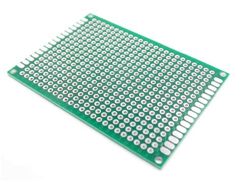
A PCB prototype is a preliminary version of a printed circuit board that is used for testing and validation purposes. It is a physical representation of the PCB design, which includes all the components, traces, and vias. PCB Prototypes are typically made in small quantities, usually one to a few pieces, to minimize costs and speed up the development process.
Why is PCB Prototyping Important?
PCB prototyping is crucial for several reasons:
-
Design Validation: PCB prototypes allow designers to test and validate their designs in real-world conditions. This helps identify any issues or errors in the design before mass production, saving time and money.
-
Functionality Testing: With a physical prototype, engineers can test the functionality of the circuit and ensure that it performs as expected. This includes testing the power supply, signal integrity, and overall performance of the PCB.
-
Optimization: PCB prototyping allows designers to optimize their designs based on the results of the testing phase. This may involve making changes to the component placement, trace routing, or other aspects of the design to improve performance, reduce costs, or enhance manufacturability.
-
Manufacturability Assessment: PCB prototypes can be used to assess the manufacturability of the design. This includes checking for any issues with the component placement, soldermask, silkscreen, or other aspects of the PCB that may affect the manufacturing process.
The PCB Prototyping Process
The PCB prototyping process typically involves the following steps:
-
Design: The first step is to create the PCB design using a CAD (Computer-Aided Design) tool. This involves creating the schematic, selecting components, and designing the PCB layout.
-
Fabrication: Once the design is finalized, the PCB prototype is fabricated. This involves creating the PCB substrate, applying the copper layers, and adding the soldermask and silkscreen.
-
Assembly: After fabrication, the components are assembled onto the PCB. This can be done manually or using automated assembly equipment, depending on the complexity of the design and the quantity of prototypes required.
-
Testing: The assembled PCB prototype is then tested to ensure that it functions as expected. This may involve using test equipment such as oscilloscopes, logic analyzers, and multimeters to measure various parameters of the circuit.
-
Optimization: Based on the results of the testing phase, the design may be optimized to improve performance, reduce costs, or enhance manufacturability.
PCB Prototyping Methods
There are several methods for creating PCB prototypes, each with its own advantages and disadvantages:
| Method | Advantages | Disadvantages |
|---|---|---|
| Etching | Low cost, can be done at home | Time-consuming, limited resolution |
| Milling | Fast turnaround, good for simple designs | Limited resolution, not suitable for complex designs |
| UV Exposure | High resolution, suitable for complex designs | Requires specialized equipment, higher cost |
| 3D Printing | Fast turnaround, suitable for unique shapes | Limited material options, lower resolution |

Benefits of Free PCB Prototyping
Many PCB manufacturers offer free PCB prototyping services to help designers and engineers test their designs without incurring significant costs. Here are some of the benefits of trying PCB prototype for free:
-
Cost Savings: Free PCB prototyping allows designers to test their designs without investing a significant amount of money. This is particularly beneficial for startups, small businesses, and individual designers who may have limited budgets.
-
Faster Time-to-Market: By using free PCB prototyping services, designers can quickly validate their designs and make any necessary changes before proceeding to mass production. This can help reduce the overall development time and bring products to market faster.
-
Risk Mitigation: Free PCB prototyping helps mitigate the risk of design errors and manufacturing issues. By testing the design with a physical prototype, designers can identify and address any problems early in the development process, reducing the risk of costly mistakes during mass production.
-
Access to Advanced Manufacturing Capabilities: Many PCB manufacturers offering free prototyping services have advanced manufacturing capabilities, such as high-density interconnect (HDI) and rigid-Flex PCBs. This allows designers to test their designs using the latest technologies and manufacturing processes, which may not be available in-house.

How to Try PCB Prototype for Free
Many PCB manufacturers offer free PCB prototyping services to attract new customers and showcase their capabilities. Here are some steps to try PCB prototype for free:
-
Research PCB Manufacturers: Look for PCB manufacturers that offer free prototyping services. Some popular options include PCBWay, JLCPCB, and OSH Park.
-
Check Eligibility Requirements: Each manufacturer may have different eligibility requirements for their free prototyping services. This may include limitations on the number of layers, PCB size, quantity, or other design parameters. Make sure your design meets these requirements before proceeding.
-
Prepare Your Design Files: To use the free prototyping service, you will need to provide your PCB design files in a format supported by the manufacturer. This typically includes Gerber files, drill files, and pick-and-place files. Ensure that your design files are complete and error-free before submitting them.
-
Submit Your Design: Follow the manufacturer’s instructions for submitting your design files. This may involve uploading the files to their website or sending them via email. Some manufacturers may also require you to create an account or provide additional information about your project.
-
Wait for Fabrication and Assembly: Once your design files have been submitted, the manufacturer will proceed with fabrication and assembly of your PCB prototype. The turnaround time may vary depending on the manufacturer and the complexity of your design, but it typically ranges from a few days to a couple of weeks.
-
Receive and Test Your Prototype: After the fabrication and assembly process is complete, the manufacturer will ship your PCB prototype to you. Upon receiving the prototype, you can proceed with testing and validation to ensure that it meets your design requirements and functions as expected.

FAQ
-
What is the difference between a PCB prototype and a production PCB?
A PCB prototype is a preliminary version of the PCB used for testing and validation, while a production PCB is the final version used for mass manufacturing. Prototypes are typically made in smaller quantities and may have different materials or manufacturing processes compared to production PCBs. -
How long does it take to receive a free PCB prototype?
The turnaround time for free PCB prototypes varies depending on the manufacturer and the complexity of the design. It can range from a few days to a couple of weeks. Most manufacturers will provide an estimated lead time when you submit your design files. -
Are there any limitations on the design of free PCB prototypes?
Yes, manufacturers offering free PCB prototyping services may have limitations on the design parameters, such as the number of layers, PCB size, or quantity. It’s essential to check the eligibility requirements of each manufacturer before submitting your design files. -
Can I use free PCB prototyping services for commercial projects?
Most manufacturers allow the use of free PCB prototyping services for commercial projects. However, it’s always a good idea to check the terms and conditions of the service to ensure that there are no restrictions on commercial use. -
What if I’m not satisfied with the quality of the free PCB prototype?
If you’re not satisfied with the quality of the free PCB prototype, contact the manufacturer and provide feedback on the issues you encountered. Most reputable manufacturers will work with you to address any problems and ensure that you’re satisfied with the final product. If the issues persist, you may need to consider alternative prototyping options or manufacturers.
Conclusion
PCB prototyping is a critical step in the development of electronic devices, allowing designers and engineers to test and validate their designs before proceeding to mass production. Free PCB prototyping services offered by many manufacturers provide an excellent opportunity to try out prototyping without incurring significant costs.
By following the steps outlined in this article, you can take advantage of free PCB prototyping services to bring your electronic design ideas to life. Remember to research manufacturers, check eligibility requirements, prepare your design files, and provide feedback on the quality of the prototype to ensure the best possible outcome for your project.
No responses yet