The History of Surface Mount Technology
The origins of surface mount technology can be traced back to the 1960s when IBM developed the first surface mount package for their System/360 computers. However, it wasn’t until the 1980s that SMT began to gain widespread adoption in the electronics industry.
The Rise of SMT in the 1980s
In the early 1980s, the electronics industry was facing a crisis. The demand for smaller, more complex devices was increasing, but the traditional through-hole technology was reaching its limits. SMT offered a solution to this problem by allowing for the production of smaller, more densely packed circuit boards.
One of the first companies to embrace SMT was Motorola, which used the technology in its popular Bravo pager in 1986. Other companies soon followed suit, and by the end of the decade, SMT had become the dominant method for producing electronic circuits.
The Advantages of SMT
There are several advantages to using surface mount technology over through-hole technology:
- Smaller size: SMT components are much smaller than through-hole components, allowing for the production of smaller, more compact devices.
- Faster assembly: SMT components can be placed on the circuit board much faster than through-hole components, which require manual insertion and soldering.
- Lower cost: SMT components are generally less expensive than through-hole components, and the faster assembly process reduces labor costs.
- Improved reliability: SMT components are less likely to be damaged during the assembly process, resulting in fewer defects and improved reliability.
The SMT Manufacturing Process
The surface mount technology manufacturing process consists of several steps:
- Solder paste application: A thin layer of solder paste is applied to the PCB using a stencil or screen printing process.
- Component placement: The SMT components are placed onto the solder paste using a pick-and-place machine.
- Reflow soldering: The PCB is heated in a reflow oven, causing the solder paste to melt and form a permanent connection between the components and the PCB.
- Inspection and testing: The assembled PCB is inspected for defects and tested to ensure proper functionality.
Solder Paste Application
The solder paste application process is critical to the success of the SMT manufacturing process. The solder paste must be applied evenly and accurately to ensure proper component placement and soldering.
There are two main methods for applying solder paste:
- Stencil printing: A stencil with holes corresponding to the component pads on the PCB is placed over the board, and solder paste is applied using a squeegee.
- Screen printing: A screen with a mesh pattern corresponding to the component pads on the PCB is placed over the board, and solder paste is applied using a squeegee.
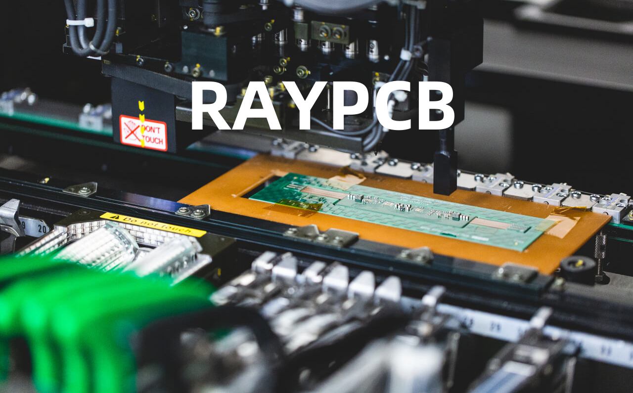
Component Placement
Once the solder paste has been applied, the SMT components are placed onto the PCB using a pick-and-place machine. These machines use computer vision and precision robotics to accurately place the components onto the solder paste.
There are two main types of pick-and-place machines:
- Chip shooters: These machines are designed for high-speed placement of smaller SMT components, such as resistors and capacitors.
- Fine pitch placers: These machines are designed for precise placement of larger SMT components, such as integrated circuits and connectors.
Reflow Soldering
After the components have been placed, the PCB is heated in a reflow oven to melt the solder paste and form a permanent connection between the components and the PCB.
The reflow soldering process typically consists of four stages:
- Preheat: The PCB is gradually heated to activate the flux in the solder paste and remove any moisture from the board.
- Soak: The temperature is held steady to allow the components to reach thermal equilibrium and the flux to remove any oxides from the component leads and PCB pads.
- Reflow: The temperature is increased to the melting point of the solder, causing it to melt and form a permanent connection between the components and the PCB.
- Cool down: The PCB is cooled to allow the solder to solidify and form a strong, reliable connection.
Inspection and Testing
After the reflow soldering process is complete, the assembled PCB is inspected for defects and tested to ensure proper functionality.
There are several methods for inspecting and testing SMT assemblies:
- Visual inspection: The assembled PCB is visually inspected for defects such as bridging, tombstoning, and insufficient solder.
- Automated optical inspection (AOI): An automated camera system is used to inspect the PCB for defects.
- X-ray inspection: X-ray imaging is used to inspect for defects that may not be visible on the surface, such as voids in the solder joints.
- In-circuit testing (ICT): The assembled PCB is tested for proper functionality using a bed-of-nails fixture that makes electrical contact with the board.
- Functional testing: The assembled PCB is tested in its final application to ensure proper functionality.

SMT Component Packages
Surface mount technology has led to the development of a wide range of component packages designed specifically for SMT Assembly. These packages are smaller and more compact than through-hole packages, allowing for the production of smaller, more densely packed devices.
Some common SMT component packages include:
Chip Components
Chip components are the smallest and most basic SMT packages. They are rectangular in shape and have two terminals, one on each end. Common chip components include resistors, capacitors, and inductors.
| Package | Dimensions (mm) | Pitch (mm) |
|---|---|---|
| 0201 | 0.6 x 0.3 | 0.3 |
| 0402 | 1.0 x 0.5 | 0.5 |
| 0603 | 1.6 x 0.8 | 0.8 |
| 0805 | 2.0 x 1.25 | 1.25 |
| 1206 | 3.2 x 1.6 | 1.6 |
Small Outline Packages (SOP)
Small outline packages are rectangular packages with leads on two sides. They are commonly used for integrated circuits and other active components.
| Package | Dimensions (mm) | Lead Count |
|---|---|---|
| SOIC | 3.9 x 1.75 | 8 – 28 |
| TSOP | 5.0 x 1.27 | 32 – 48 |
| TSSOP | 4.4 x 2.65 | 8 – 64 |
| SSOP | 5.3 x 6.2 | 16 – 56 |
Quad Flat Packages (QFP)
Quad flat packages are square packages with leads on all four sides. They are commonly used for microcontrollers and other complex integrated circuits.
| Package | Dimensions (mm) | Lead Count |
|---|---|---|
| LQFP | 7.0 x 7.0 | 32 – 100 |
| TQFP | 10.0 x 10.0 | 32 – 176 |
| QFN | 4.0 x 4.0 | 16 – 68 |
Ball Grid Array (BGA)
Ball grid array packages are square packages with a grid of solder balls on the bottom. They are commonly used for high-density integrated circuits such as microprocessors and FPGAs.
| Package | Dimensions (mm) | Ball Count |
|---|---|---|
| PBGA | 15.0 x 15.0 | 119 – 1521 |
| FBGA | 13.0 x 13.0 | 256 – 1156 |
| VFBGA | 8.0 x 8.0 | 100 – 450 |

The Future of Surface Mount Technology
Surface mount technology has revolutionized the electronics industry, enabling the production of smaller, faster, and more efficient devices. As the demand for even smaller and more complex devices continues to grow, SMT will continue to evolve to meet these challenges.
Trends in SMT
Some of the key trends shaping the future of surface mount technology include:
- Miniaturization: As devices continue to shrink in size, SMT component packages will need to become even smaller and more compact.
- Increased functionality: As devices become more complex, SMT assemblies will need to incorporate a wider range of components and functions.
- Higher density: As the demand for smaller devices grows, SMT assemblies will need to become more densely packed, with more components per square inch.
- Advanced materials: New materials, such as advanced ceramics and composites, will be needed to meet the demands of miniaturization and increased functionality.
Challenges and Opportunities
While surface mount technology has come a long way since its early days, there are still many challenges and opportunities ahead. Some of the key challenges facing the SMT industry include:
- Increasing complexity: As devices become more complex, SMT assemblies will need to incorporate a wider range of components and functions, which can increase the risk of defects and failures.
- Environmental concerns: The use of lead-based solders and other hazardous materials in SMT assembly is coming under increasing scrutiny, and the industry will need to find safer and more sustainable alternatives.
- Supply chain disruptions: The COVID-19 pandemic has highlighted the vulnerability of global supply chains, and the SMT industry will need to find ways to build more resilient and flexible supply chains in the future.
At the same time, there are also many opportunities for innovation and growth in the SMT industry. Some of the key opportunities include:
- Internet of Things (IoT): The growing demand for connected devices is driving demand for smaller, more efficient SMT assemblies.
- 5G networks: The rollout of 5G networks is creating new opportunities for SMT assemblies in applications such as smartphones, base stations, and IoT devices.
- Automotive electronics: The increasing use of electronics in vehicles is driving demand for high-reliability SMT assemblies that can withstand harsh environments.
- Medical devices: The growing demand for smaller, more portable medical devices is driving demand for advanced SMT assemblies that can incorporate complex functions in a small footprint.

Frequently Asked Questions (FAQ)
Q: What is the difference between surface mount technology (SMT) and through-hole technology (THT)?
A: SMT components are mounted directly onto the surface of the PCB, while THT components have leads that are inserted into holes drilled through the PCB. SMT allows for smaller, more compact assemblies, while THT is often used for larger components or in applications where mechanical strength is important.
Q: What are the advantages of using SMT over THT?
A: SMT offers several advantages over THT, including smaller size, faster assembly, lower cost, and improved reliability. SMT components are also easier to automate, which reduces labor costs and improves consistency.
Q: What are some common defects in SMT assembly?
A: Some common defects in SMT assembly include bridging (solder connecting adjacent pads), tombstoning (components standing up on end), insufficient solder, and solder balls. These defects can be caused by issues with the solder paste application, component placement, or reflow soldering process.
Q: What is the role of solder paste in SMT assembly?
A: Solder paste is a mixture of solder particles and flux that is applied to the PCB before the components are placed. The solder paste holds the components in place during the reflow soldering process and forms a permanent electrical and mechanical connection between the components and the PCB.
Q: What is the future of surface mount technology?
A: The future of SMT is likely to be driven by trends such as miniaturization, increased functionality, higher density, and advanced materials. As devices continue to shrink in size and become more complex, SMT will need to evolve to meet these challenges. At the same time, there are also many opportunities for innovation and growth in areas such as IoT, 5G networks, automotive electronics, and medical devices.
No responses yet