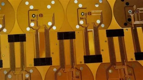
What is a Flexible PCB?
A flexible printed circuit board (PCB), also known as a flex circuit, is a type of PCB that consists of a thin, flexible plastic substrate with printed circuitry. Unlike traditional rigid PCBs, flexible PCBs can bend, twist, and fold to fit into tight spaces or conform to specific shapes. This makes them ideal for applications where space is limited, or where the PCB needs to move or flex during operation.
Flexible PCBs are commonly used in a wide range of industries, including:
- Consumer electronics (smartphones, wearables, etc.)
- Medical devices (hearing aids, pacemakers, etc.)
- Automotive (dashboard displays, sensors, etc.)
- Aerospace (avionics, satellite systems, etc.)
- Industrial equipment (robotics, machine control, etc.)
The flexibility of these PCBs is achieved by using a thin, flexible substrate material, such as polyimide (PI) or polyester (PET). The circuitry is then printed onto this substrate using conductive inks or traces, typically made of copper. The thickness of the substrate and the copper traces can vary depending on the application and the required level of flexibility.
Advantages of Flexible PCBs
Flexible PCBs offer several advantages over traditional rigid PCBs:
-
Space savings: Flexible PCBs can be bent, folded, or shaped to fit into tight spaces, allowing for more compact and lightweight designs.
-
Increased reliability: The flexibility of the PCB reduces stress on components and solder joints, improving the overall reliability of the device.
-
Improved signal integrity: Flexible PCBs can be designed with shorter signal paths, reducing signal loss and improving signal integrity.
-
Enhanced durability: Flexible PCBs can withstand repeated bending and flexing without damage, making them suitable for applications where motion or vibration is present.
-
Cost-effective: In some cases, using a flexible PCB can reduce the overall cost of a device by eliminating the need for separate connectors and wiring.

Types of Flexible PCBs
There are three main types of flexible PCBs:
-
Single-sided flexible PCBs: These PCBs have conductive traces on only one side of the substrate. They are the simplest and most cost-effective type of flexible PCB.
-
Double-sided flexible PCBs: These PCBs have conductive traces on both sides of the substrate, allowing for more complex circuitry and higher component density.
-
Multi-layer flexible PCBs: These PCBs consist of multiple layers of flexible substrate with conductive traces, separated by insulating layers. They offer the highest level of complexity and density but are also the most expensive to manufacture.
Additionally, flexible PCBs can be categorized based on their construction:
-
Adhesiveless flexible PCBs: These PCBs do not use adhesive to bond the copper traces to the substrate, resulting in a thinner and more flexible PCB.
-
Adhesive-based flexible PCBs: These PCBs use an adhesive layer to bond the copper traces to the substrate, providing better adhesion but slightly reducing flexibility.
-
Rigid-Flex PCBs: These hybrid PCBs combine rigid and flexible sections, allowing for the integration of both types of circuitry in a single board.

Flexible PCB Manufacturing Process
The manufacturing process for flexible PCBs is similar to that of rigid PCBs, but with some key differences to account for the unique properties of the flexible substrate. The main steps in the flexible PCB manufacturing process are:
-
Substrate preparation: The flexible substrate material, typically polyimide or polyester, is cleaned and treated to ensure proper adhesion of the conductive traces.
-
Copper lamination: A thin layer of copper is laminated onto the substrate using heat and pressure. The copper can be pre-formed or sputtered onto the substrate.
-
Circuit patterning: The desired circuit pattern is transferred onto the copper layer using a photolithographic process. This involves applying a photoresist coating, exposing it to UV light through a patterned mask, and then developing the resist to remove the unexposed areas.
-
Etching: The exposed copper is etched away using a chemical solution, leaving behind the desired circuit pattern.
-
Protective coating: A protective cover layer, typically a coverlay or solder mask, is applied over the circuitry to insulate and protect it from damage.
-
Drilling and cutting: Any necessary holes (vias) are drilled through the PCB, and the board is cut to its final shape using a laser or mechanical cutter.
-
Surface finishing: The exposed copper pads are coated with a surface finish, such as ENIG (Electroless Nickel Immersion Gold) or OSP (Organic Solderability Preservative), to prevent oxidation and improve solderability.
-
Electrical testing: The completed flexible PCB is tested for continuity, shorts, and other electrical properties to ensure it meets the required specifications.
| Step | Description |
|---|---|
| 1 | Substrate preparation |
| 2 | Copper lamination |
| 3 | Circuit patterning |
| 4 | Etching |
| 5 | Protective coating |
| 6 | Drilling and cutting |
| 7 | Surface finishing |
| 8 | Electrical testing |

Design Considerations for Flexible PCBs
Designing a flexible PCB requires careful consideration of several factors to ensure the board’s reliability and performance. Some key design considerations include:
-
Bend radius: The minimum bend radius of the flexible PCB must be determined based on the substrate material, copper thickness, and the number of layers. Exceeding the minimum bend radius can cause damage to the circuitry.
-
Copper thickness: Thinner copper traces are more flexible but have higher resistance and lower current-carrying capacity. Thicker traces are less flexible but offer better electrical performance.
-
Adhesive selection: The adhesive used to bond the copper to the substrate must be compatible with the substrate material and provide adequate adhesion without compromising flexibility.
-
Coverlay and stiffeners: Coverlay and stiffeners can be used to reinforce specific areas of the flexible PCB, such as connector locations or areas subject to higher stress.
-
Trace routing: Traces should be routed to minimize stress during bending, typically by running them perpendicular to the bend direction. Avoid sharp corners and use curved traces where possible.
-
Component placement: Components should be placed in areas of the flexible PCB that experience minimal bending or flexing to reduce stress on the solder joints.
-
Strain relief: Strain relief features, such as slits or cut-outs, can be incorporated into the design to reduce stress concentration at specific points and improve the overall flexibility of the PCB.
Applications of Flexible PCBs
Flexible PCBs are used in a wide range of applications across various industries. Some common applications include:
-
Wearable devices: Smartwatches, fitness trackers, and other wearable electronics rely on flexible PCBs to achieve compact, lightweight, and comfortable designs.
-
Medical implants: Pacemakers, cochlear implants, and other medical implants use flexible PCBs to conform to the shape of the human body and withstand constant flexing and movement.
-
Automotive electronics: Flexible PCBs are used in automotive applications, such as instrument clusters, sensors, and entertainment systems, where space is limited and reliability is critical.
-
Aerospace and defense: Flexible PCBs are used in avionics, satellite systems, and military equipment due to their ability to withstand vibration, shock, and extreme temperatures.
-
Industrial automation: Robotics, machine control systems, and other industrial equipment use flexible PCBs to enable compact designs and improve reliability in harsh environments.
-
Consumer electronics: Smartphones, tablets, and laptops often use flexible PCBs for connecting displays, keyboards, and other components, allowing for slimmer and more compact designs.
Challenges in Flexible PCB Manufacturing
While flexible PCBs offer numerous benefits, their manufacturing process presents some unique challenges compared to traditional rigid PCBs:
-
Material handling: The thin, flexible substrates used in flexible PCBs can be difficult to handle during the manufacturing process, requiring specialized equipment and techniques to prevent damage or distortion.
-
Adhesion: Ensuring proper adhesion between the copper traces and the flexible substrate is critical for the reliability and durability of the PCB. Poor adhesion can lead to delamination and circuit failures.
-
Dimensional stability: Flexible substrates can expand or contract during the manufacturing process, making it challenging to maintain tight tolerances and precise circuit patterns.
-
Coverlay alignment: Aligning and laminating the coverlay onto the flexible PCB requires precision to ensure proper insulation and protection of the circuitry.
-
Testing and inspection: Flexible PCBs can be more difficult to test and inspect than rigid PCBs due to their flexibility and the potential for damage during handling.
-
Cost: Flexible PCBs typically have higher material and manufacturing costs compared to rigid PCBs due to the specialized substrates, processes, and equipment required.
Despite these challenges, advancements in materials, manufacturing technologies, and design tools have made flexible PCB manufacturing more accessible and cost-effective in recent years. As the demand for compact, lightweight, and flexible electronics continues to grow, the use of flexible PCBs is expected to increase across various industries.
Frequently Asked Questions (FAQ)
-
Q: What is the typical thickness of a flexible PCB?
A: The thickness of a flexible PCB can vary depending on the application and design requirements. Single-layer flexible PCBs can be as thin as 0.05mm, while multi-layer boards can range from 0.2mm to 2mm or more. -
Q: Can flexible PCBs be soldered using standard methods?
A: Yes, flexible PCBs can be soldered using standard methods such as reflow soldering, Wave Soldering, and hand soldering. However, care must be taken to avoid excessive heat or mechanical stress that could damage the flexible substrate or components. -
Q: How long do flexible PCBs last compared to rigid PCBs?
A: The lifespan of a flexible PCB depends on various factors, such as the materials used, the application environment, and the level of stress and flexing experienced. In general, a well-designed and manufactured flexible PCB can last as long as a rigid PCB in similar conditions, often several years or more. -
Q: Are flexible PCBs more expensive than rigid PCBs?
A: Yes, flexible PCBs are typically more expensive than rigid PCBs due to the specialized materials, processes, and equipment required for their manufacture. However, the cost difference can be justified in applications where the benefits of flexibility, such as space savings, reliability, and durability, are critical. -
Q: Can flexible PCBs be used in high-temperature applications?
A: Yes, certain types of flexible PCBs can be designed to withstand high temperatures. Polyimide (PI) is a common substrate material for high-temperature applications, as it can withstand temperatures up to 300°C. However, the design and manufacturing process must take into account the thermal expansion and other properties of the materials used.
No responses yet