Identify the Problem
The first step in PCB Repair is to identify the problem. This can be done through visual inspection and diagnostic tests.
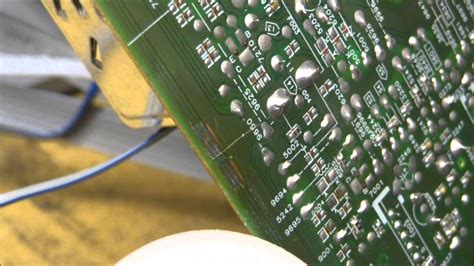
Visual Inspection
Begin by visually inspecting the PCB for any obvious signs of damage, such as:
- Burned or discolored components
- Cracked or broken traces
- Corroded or damaged solder joints
- Physical damage to the board itself
Diagnostic Tests
If the problem is not visually apparent, you may need to perform diagnostic tests to pinpoint the issue. Some common diagnostic methods include:
- Continuity testing: Using a multimeter to check for continuity between various points on the PCB
- Power supply testing: Ensuring that the PCB is receiving the correct voltage and current
- Signal tracing: Following the path of a signal through the PCB to identify where it may be interrupted or distorted
Clean the PCB
Before attempting any repairs, it is crucial to clean the PCB thoroughly. Dirt, dust, and other contaminants can interfere with the repair process and cause further damage.
Cleaning Methods
There are several methods for cleaning PCBs, depending on the type and extent of contamination:
- Isopropyl alcohol: Use a soft brush or cloth dampened with isopropyl alcohol to gently remove dirt and grime from the PCB surface.
- Ultrasonic cleaning: For more stubborn contamination, an ultrasonic cleaner can be used to agitate a cleaning solution and remove debris from hard-to-reach areas.
- Compressed air: Use compressed air to blow away loose particles and dust from the PCB surface and components.
Safety Precautions
When cleaning PCBs, always take appropriate safety precautions:
- Wear protective gloves and eyewear to avoid contact with cleaning solutions and debris
- Work in a well-ventilated area to avoid inhaling fumes from cleaning agents
- Ensure the PCB is completely dry before applying power or attempting repairs

Repair Damaged Components
Once the PCB is clean and the problem has been identified, the next step is to repair or replace any damaged components.
Soldering Techniques
Soldering is a essential skill for PCB repair. When repairing or replacing components, keep these soldering tips in mind:
- Use a temperature-controlled soldering iron with an appropriately sized tip
- Apply heat to the component lead and PCB pad simultaneously to ensure a good solder joint
- Use flux to improve solder flow and prevent oxidation
- Avoid applying excessive heat, which can damage components or lift PCB pads
Component Replacement
If a component is damaged beyond repair, it will need to be replaced. Follow these steps for successful component replacement:
- Carefully desolder the damaged component, using solder wick or a desoldering pump to remove excess solder
- Clean the component pads on the PCB to ensure good contact with the new component
- Place the new component in position, ensuring correct orientation and alignment
- Solder the new component in place, applying heat evenly to the leads and pads

Repair Damaged Traces
PCB Traces can become damaged due to physical stress, overheating, or corrosion. Repairing damaged traces is a delicate process that requires patience and precision.
Trace Repair Methods
There are several methods for repairing damaged PCB traces, depending on the extent of the damage:
- Jumper wires: For small breaks in traces, a thin insulated wire can be soldered across the break to restore continuity.
- Conductive epoxy: Conductive epoxy can be used to fill in gaps or strengthen weakened traces. Apply the epoxy carefully and allow it to cure fully before applying power.
- Trace repair pens: Specialized trace repair pens contain conductive ink that can be used to draw new traces over damaged areas. Multiple layers may be needed to achieve the desired conductivity.
Insulation Considerations
When repairing traces, it is important to consider insulation to prevent short circuits:
- Use insulated jumper wires or apply insulating coatings over repaired traces
- Ensure adequate spacing between repaired traces and adjacent components or traces
- Test for short circuits before applying power to the repaired PCB

Protect the Repaired PCB
After completing repairs, it is essential to protect the PCB from further damage.
Conformal Coatings
Conformal coatings are thin, protective layers applied over the PCB surface to shield it from moisture, dust, and other environmental hazards. Common conformal coating materials include:
- Acrylic: Offers good moisture and abrasion resistance, easy to apply and remove
- Silicone: Provides excellent temperature and chemical resistance, but can be difficult to remove for future repairs
- Urethane: Offers the highest level of protection against moisture and chemicals, but can be expensive and difficult to apply
Enclosures
Placing the repaired PCB in a suitable enclosure can provide additional protection against physical damage and environmental factors. When selecting an enclosure, consider:
- Material: Plastic, metal, or composite materials offer different levels of durability and shielding properties
- Size: Ensure the enclosure is large enough to accommodate the PCB and any connected components or wires
- Mounting: Choose an enclosure with appropriate mounting options for your application, such as screw mounts, snap fits, or DIN rail compatibility
Test and Verify Repairs
The final step in PCB repair is to test and verify that the repairs have been successful and the PCB is functioning as intended.
Power-on Testing
Before applying full power to the repaired PCB, it is a good idea to perform a low-power test to check for any immediate issues:
- Connect the PCB to a current-limited power supply set to a low voltage
- Gradually increase the voltage while monitoring for any signs of overheating, smoke, or unusual behavior
- If the low-power test is successful, proceed to apply full power and test the PCB’s functionality
Functional Testing
Once the PCB is powered on, perform a thorough functional test to ensure it is operating correctly:
- Test all inputs and outputs to verify proper operation
- Exercise any special functions or modes of the PCB
- Use test equipment such as oscilloscopes or logic analyzers to monitor signals and check for any anomalies
Stress Testing
To ensure the repaired PCB will hold up under real-world conditions, it is a good idea to perform stress testing:
- Thermal cycling: Subject the PCB to repeated cycles of heating and cooling to check for any weaknesses in solder joints or components
- Vibration testing: Use a vibration table or shaker to simulate the effects of mechanical stress on the PCB
- Burn-in testing: Operate the PCB continuously for an extended period to identify any components prone to early failure
By following these six tips for PCB repair, you can effectively diagnose, repair, and protect Printed Circuit Boards, saving time and money compared to full board replacement. As with any electronics repair work, always prioritize safety and take the necessary precautions to avoid injury or further damage to the equipment.
Frequently Asked Questions (FAQ)
1. What tools do I need for PCB repair?
Some essential tools for PCB repair include:
- Soldering iron and solder
- Solder wick and desoldering pump
- Multimeter and oscilloscope
- Tweezers, pliers, and cutters
- Magnifying glass or microscope
- Isopropyl alcohol and cleaning brushes
2. Can I repair a PCB without a schematic diagram?
While a schematic diagram is helpful for understanding the circuit and identifying components, it is possible to repair a PCB without one. You will need to rely on visual inspection, continuity testing, and your knowledge of electronic components and circuits to diagnose and repair the board.
3. How do I identify the value of a damaged component?
If the component markings are not visible or the component is too damaged to identify, you can try these methods:
- Consult the schematic diagram or bill of materials (BOM) for the PCB, if available
- Measure the component with a multimeter and compare the values to known Component Types
- Look for similar components on the same PCB or on a reference board and measure their values
4. Can I use regular solder for PCB repair?
While regular solder can be used for PCB repair, it is recommended to use solder specifically designed for electronics work. Lead-free solder is preferred for environmental and health reasons, but leaded solder may be necessary for certain applications or older PCBs.
5. How do I prevent static damage when repairing PCBs?
To prevent static damage to sensitive components during PCB repair:
- Wear an anti-static wrist strap or work on an anti-static mat
- Avoid touching component leads or PCB traces directly with your fingers
- Store sensitive components in anti-static bags when not in use
- Use grounded, temperature-controlled soldering irons to avoid static buildup
By understanding these common questions and their answers, you can be better prepared to tackle PCB repair projects and achieve successful outcomes.
No responses yet