Introduction to PCB Tools
Printed Circuit Board (PCB) design and manufacturing is a complex process that requires specialized tools for programming and testing. These PCB tools are essential for ensuring the functionality, reliability, and quality of the final product. In this article, we will explore 11 crucial aspects of PCB programming and testing tools that every engineer and manufacturer should be aware of.
1. PCB Design Software
1.1. Overview of PCB Design Software
PCB design software is the foundation of the PCB development process. These tools allow engineers to create schematic diagrams, design PCB layouts, and generate manufacturing files. Some popular PCB design software include:
- Altium Designer
- Eagle
- KiCad
- OrCAD
- Mentor Graphics PADS
1.2. Key Features of PCB Design Software
PCB design software typically offers the following key features:
- Schematic capture
- PCB layout design
- Component library management
- Design rule checking (DRC)
- 3D visualization
- Gerber and drill file generation
1.3. Choosing the Right PCB Design Software
When selecting a PCB design software, consider the following factors:
- Ease of use
- Compatibility with other tools
- Library and component support
- Pricing and licensing
- Community support and resources

2. PCB Simulation Tools
2.1. Importance of PCB Simulation
PCB simulation tools allow engineers to verify the functionality and performance of their designs before manufacturing. This helps to identify and resolve issues early in the development process, reducing the risk of costly mistakes and redesigns.
2.2. Types of PCB Simulation Tools
There are several types of PCB simulation tools, including:
- SPICE (Simulation Program with Integrated Circuit Emphasis)
- Finite Element Analysis (FEA)
- Electromagnetic Compatibility (EMC) simulation
- Thermal simulation
- Signal integrity analysis
2.3. Benefits of Using PCB Simulation Tools
PCB simulation tools offer numerous benefits, such as:
- Identifying design flaws early
- Optimizing performance and functionality
- Reducing development time and costs
- Improving product reliability and quality

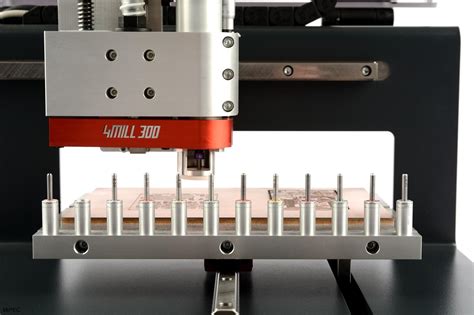
3. PCB Prototyping and Manufacturing
3.1. PCB Prototyping Methods
PCB prototyping is the process of creating a physical representation of the PCB design for testing and validation. Common PCB prototyping methods include:
- Breadboarding
- Perfboard assembly
- Milling and routing
- 3D printing
3.2. PCB Manufacturing Processes
Once the PCB design is finalized, it enters the manufacturing stage. PCB manufacturing processes typically involve the following steps:
- PCB fabrication (etching, drilling, plating)
- Component placement (SMT, THT)
- Soldering (reflow, wave)
- Inspection and testing
3.3. Choosing a PCB Manufacturer
When selecting a PCB manufacturer, consider the following factors:
- Manufacturing capabilities (layer count, material options, etc.)
- Quality control processes
- Turnaround time
- Pricing and minimum order quantities (MOQs)
- Customer support and communication

4. PCB Testing Equipment
4.1. Overview of PCB Testing Equipment
PCB testing equipment is used to verify the functionality, performance, and reliability of manufactured PCBs. Some common types of PCB testing equipment include:
- Multimeters
- Oscilloscopes
- Logic analyzers
- In-circuit testers (ICT)
- Flying probe testers
- Boundary scan testers
4.2. Choosing the Right PCB Testing Equipment
When selecting PCB testing equipment, consider the following factors:
- Testing requirements (functionality, performance, etc.)
- Compatibility with PCB design and components
- Automation capabilities
- Ease of use and programming
- Cost and maintenance
5. PCB Programming Tools
5.1. Overview of PCB Programming Tools
PCB programming tools are used to write firmware and software for the components on a PCB, such as microcontrollers, FPGAs, and CPLDs. Some popular PCB programming tools include:
- Integrated Development Environments (IDEs)
- Arduino IDE
- MPLAB X
- IAR Embedded Workbench
- Programmers and debuggers
- JTAG
- SWD (Serial Wire Debug)
- ICSP (In-Circuit Serial Programming)
5.2. Choosing the Right PCB Programming Tools
When selecting PCB programming tools, consider the following factors:
- Compatibility with target device (microcontroller, FPGA, etc.)
- Supported programming languages (C, C++, Assembly, etc.)
- Debugging capabilities
- Integration with other development tools
- Community support and resources
6. PCB Debugging Techniques
6.1. Common PCB Debugging Techniques
PCB debugging is the process of identifying and resolving issues with a PCB design or manufactured board. Some common PCB debugging techniques include:
- Visual inspection
- Continuity testing
- Voltage and current measurements
- Signal tracing
- Thermal imaging
- In-circuit emulation (ICE)
6.2. Best Practices for PCB Debugging
To effectively debug PCBs, follow these best practices:
- Use a systematic approach (divide and conquer)
- Document findings and changes
- Utilize appropriate testing equipment
- Collaborate with team members
- Continuously improve debugging skills
7. PCB Version Control and Collaboration
7.1. Importance of Version Control for PCB Projects
Version control is essential for managing changes and revisions in PCB projects. It allows teams to:
- Track changes and history
- Collaborate effectively
- Revert to previous versions if needed
- Manage branches and merges
7.2. Version Control Systems for PCB Projects
Some popular version control systems for PCB projects include:
- Git
- SVN (Subversion)
- Perforce
- Altium Vault
7.3. Best Practices for PCB Project Collaboration
To foster effective collaboration in PCB projects, follow these best practices:
- Establish clear communication channels
- Define roles and responsibilities
- Use a centralized repository for version control
- Implement a structured workflow (e.g., feature branches, pull requests)
- Regularly review and provide feedback on changes
8. PCB Design for Manufacturing (DFM)
8.1. Overview of PCB Design for Manufacturing
PCB Design for Manufacturing (DFM) is the practice of designing PCBs with manufacturing considerations in mind. This helps to ensure that the PCB can be efficiently and reliably manufactured, reducing the risk of defects and delays.
8.2. Key Aspects of PCB DFM
Some key aspects of PCB DFM include:
- Component selection and placement
- Trace routing and spacing
- Solder mask and silkscreen design
- Panelization and break-away tabs
- Testability and accessibility
8.3. Benefits of Implementing PCB DFM
Implementing PCB DFM offers several benefits, such as:
- Improved manufacturability and yield
- Reduced production time and costs
- Enhanced product quality and reliability
- Faster time-to-market
9. PCB Design for Testing (DFT)
9.1. Overview of PCB Design for Testing
PCB Design for Testing (DFT) is the practice of designing PCBs with testing considerations in mind. This helps to ensure that the PCB can be efficiently and thoroughly tested, reducing the risk of defects and failures in the field.
9.2. Key Aspects of PCB DFT
Some key aspects of PCB DFT include:
- Test point placement and accessibility
- Boundary scan chain design
- Built-in self-test (BIST) features
- Diagnostic interfaces (JTAG, I2C, etc.)
- Testability analysis and optimization
9.3. Benefits of Implementing PCB DFT
Implementing PCB DFT offers several benefits, such as:
- Improved testability and fault coverage
- Reduced testing time and costs
- Enhanced product quality and reliability
- Easier maintenance and troubleshooting
10. PCB Standards and Regulations
10.1. Overview of PCB Standards and Regulations
PCB design and manufacturing must adhere to various standards and regulations to ensure safety, compatibility, and compliance. Some common PCB standards and regulations include:
- IPC (Association Connecting Electronics Industries)
- IPC-2221: Generic Standard on Printed Board Design
- IPC-6012: Qualification and Performance Specification for Rigid Printed Boards
- UL (Underwriters Laboratories)
- RoHS (Restriction of Hazardous Substances)
- REACH (Registration, Evaluation, Authorization, and Restriction of Chemicals)
10.2. Importance of Complying with PCB Standards and Regulations
Complying with PCB standards and regulations is crucial for:
- Ensuring product safety and reliability
- Meeting customer and market requirements
- Avoiding legal and financial consequences
- Facilitating global trade and compatibility
10.3. Best Practices for Ensuring Compliance
To ensure compliance with PCB standards and regulations, follow these best practices:
- Stay informed about relevant standards and regulations
- Incorporate compliance requirements into the design process
- Use compliant materials and components
- Maintain accurate documentation and records
- Regularly audit and review compliance status
11. Continuous Learning and Skill Development
11.1. Importance of Continuous Learning in PCB Industry
The PCB industry is constantly evolving, with new technologies, techniques, and tools emerging regularly. To stay competitive and effective, engineers and manufacturers must continuously learn and develop their skills.
11.2. Resources for PCB Learning and Skill Development
Some valuable resources for PCB learning and skill development include:
- Online courses and tutorials (Udemy, Coursera, YouTube)
- Industry conferences and workshops (PCB West, IPC APEX EXPO)
- Professional organizations (IPC, IEEE)
- Technical books and publications
- PCB design and manufacturing communities (forums, social media groups)
11.3. Best Practices for Continuous Learning and Skill Development
To foster continuous learning and skill development, follow these best practices:
- Set learning goals and create a development plan
- Allocate time and resources for learning activities
- Engage with industry peers and experts
- Participate in hands-on projects and experiments
- Share knowledge and experiences with others
Conclusion
PCB programming and testing tools are essential for designing, manufacturing, and validating high-quality and reliable PCBs. By understanding the various aspects of these tools, including PCB design software, simulation tools, prototyping and manufacturing processes, testing equipment, programming tools, debugging techniques, version control and collaboration, DFM, DFT, standards and regulations, and continuous learning, engineers and manufacturers can optimize their PCB development workflow and deliver superior products.
FAQs
- What is the difference between PCB design software and PCB simulation tools?
-
PCB design software is used for creating schematic diagrams, designing PCB layouts, and generating manufacturing files, while PCB simulation tools are used for verifying the functionality and performance of the design before manufacturing.
-
Why is PCB Design for Manufacturing (DFM) important?
-
PCB DFM is important because it helps to ensure that the PCB can be efficiently and reliably manufactured, reducing the risk of defects, delays, and costs, while improving product quality and time-to-market.
-
What are some common PCB testing equipment?
-
Some common PCB testing equipment include multimeters, oscilloscopes, logic analyzers, in-circuit testers (ICT), flying probe testers, and boundary scan testers.
-
How does version control benefit PCB projects?
-
Version control benefits PCB projects by allowing teams to track changes and history, collaborate effectively, revert to previous versions if needed, and manage branches and merges, ensuring a more organized and efficient development process.
-
Why is continuous learning important in the PCB industry?
- Continuous learning is important in the PCB industry because it helps engineers and manufacturers stay competitive and effective in an ever-evolving landscape, where new technologies, techniques, and tools emerge regularly, requiring constant skill development and adaptation.
No responses yet